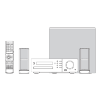
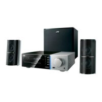
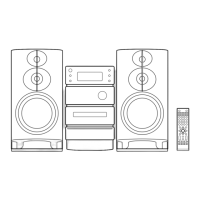
Do you have a question about the JVC NX-F7B and is the answer not in the manual?
Details the local regulator circuits for power supply management within the system.
Explains the microcontroller (MICOM) unit and its peripheral connections for system control.
Covers the first part of the audio signal processing and output circuitry.
Details the second part of the audio signal processing and output circuitry.
Presents the third part of the audio signal processing and output circuitry.
Illustrates the digital amplifier circuits responsible for audio power output.
Diagrams the front panel display (FL) and external connection jacks.
Details the video signal processing, output, and conversion circuits.
Covers the first part of the front-end signal acquisition and processing.
Details the second part of the front-end signal acquisition and processing.
Presents the third part of the front-end signal acquisition and processing.
Illustrates the fourth part of the front-end signal acquisition and processing.
Diagrams the disc loading mechanism and associated control circuits.
Shows the component placement and routing for the main printed circuit board.
Illustrates the component layout for the amplifier printed circuit board.
Depicts the component placement for the front panel printed circuit board.
Shows the layout for the voltage selection printed circuit board.
Illustrates the component placement for the front-end processing printed circuit board.
Depicts the component layout for the front jack printed circuit board.
Shows the component placement for the SCART interface printed circuit board.
Illustrates the component layout for the disc loader printed circuit board.
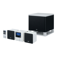
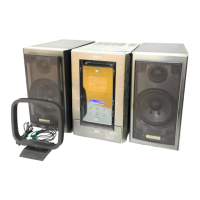
| Brand | JVC |
|---|---|
| Model | NX-F7B |
| Category | Speaker System |
| Language | English |