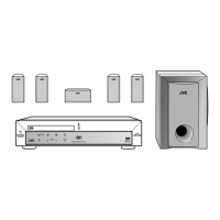
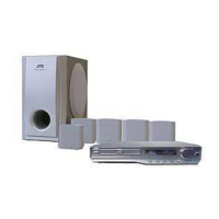
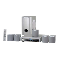
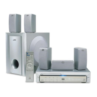
TH-A5R
1-22
1
2
3,4
5~6
7~ 8
9
10
11~14
15~16
17
18
19
20
21
22
23
24
25
26
27
28
29
30
31
32
33
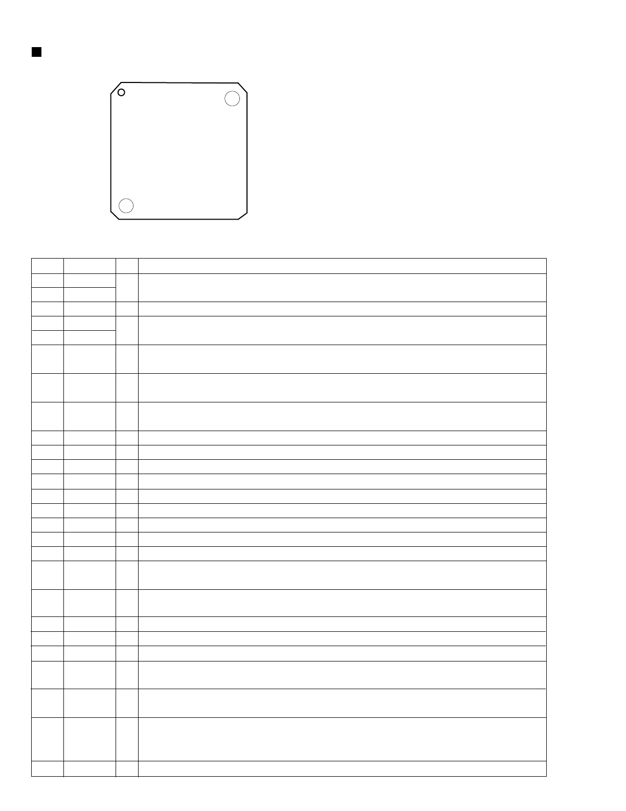
Pin No.
Symbol I/O Function
SP3721A (U7) : DVD driver
1.Pin layout
1
16
48
33
64 ~ 49
17 ~ 32
~
~
2.Pin function (1/2)
DVDRFP
DVDRFN
PD1,PD2
A2,B2
C2,D2
CP
CN
A,B,C,D
E,F
CDTE
VCI2
NC
VNB
DVDPD
DVDLD
CDPD
CDLD
LDON#
VC
VCI
VPB
MIRR
MP
MB
FDCHG#
MLPF
RF Signal Inputs. Differential RF signal attenuator input pins.
CD Photo detector Interface Inputs. Inputs from the CD photo detector error outputs.
Photo Detector Interface Inputs. AC coupled inputs for the DPD from
the main beam Photo detector matrix outputs.
Differential Phase tracking LPF pin. An external capacitance is
connected between this pin and the CN pin.
Differential Phase tracking LPF pin. An external capacitance is
connected between this pin and the CP pin.
Photo Detector Interface Inputs. Inputs from the main beam Photo
detector matrix outputs.
CD tracking Error Inputs. Inputs from the CD photo detector error outputs.
CD Tracking. E-F Opamp output for feedback.
Reference Voltage input. DC bias voltage input for the servo input reference.
No Connect.
Ground. Ground pin for the servo block.
APC Input. DVD APC input pin from the monitor photo diode.
APC output. DVD APC output pin to control the laser power.
APC Input. DVD APC input pin from the monitor photo diode.
APC output. DVD APC output pin to control the laser power.
APC output. on/off. APC output control pin. A low level activates the
LD output. (open high)
Reference Voltage output. This pin provides the internal DC bias
reference voltage (+2.5+ fix). Output impedance is less than 50 ohms.
Reference Voltage input. DC bias voltage input for the servo input reference.
Power. Power supply pin for the servo block.
Mirror Detect Output. Mirror Detect comparator output. Pseudo CMOS output.
MIRR signal Peak hold pin. An external capacitance is connected to
between this pin and VPB.
MIRR signal Bottom hold pin. An external capacitance is connected to
between this pin and VPB.
Low Impedance Enable. A TTL compatible input pin that activates the FDCHG switches.
A low level activates the switches and the falling edge of the internal FDCHG triggers
the fast decay for the NIRR bottom hold circuit. (open high)
MIRR signal LPF pin. An external capacitance is connected between this pin and VPB.
I
I
I
I/O
I/O
I
I
-
-
-
-
I
O
I
O
I
-
-
-
O
-
-
I
-
 Loading...