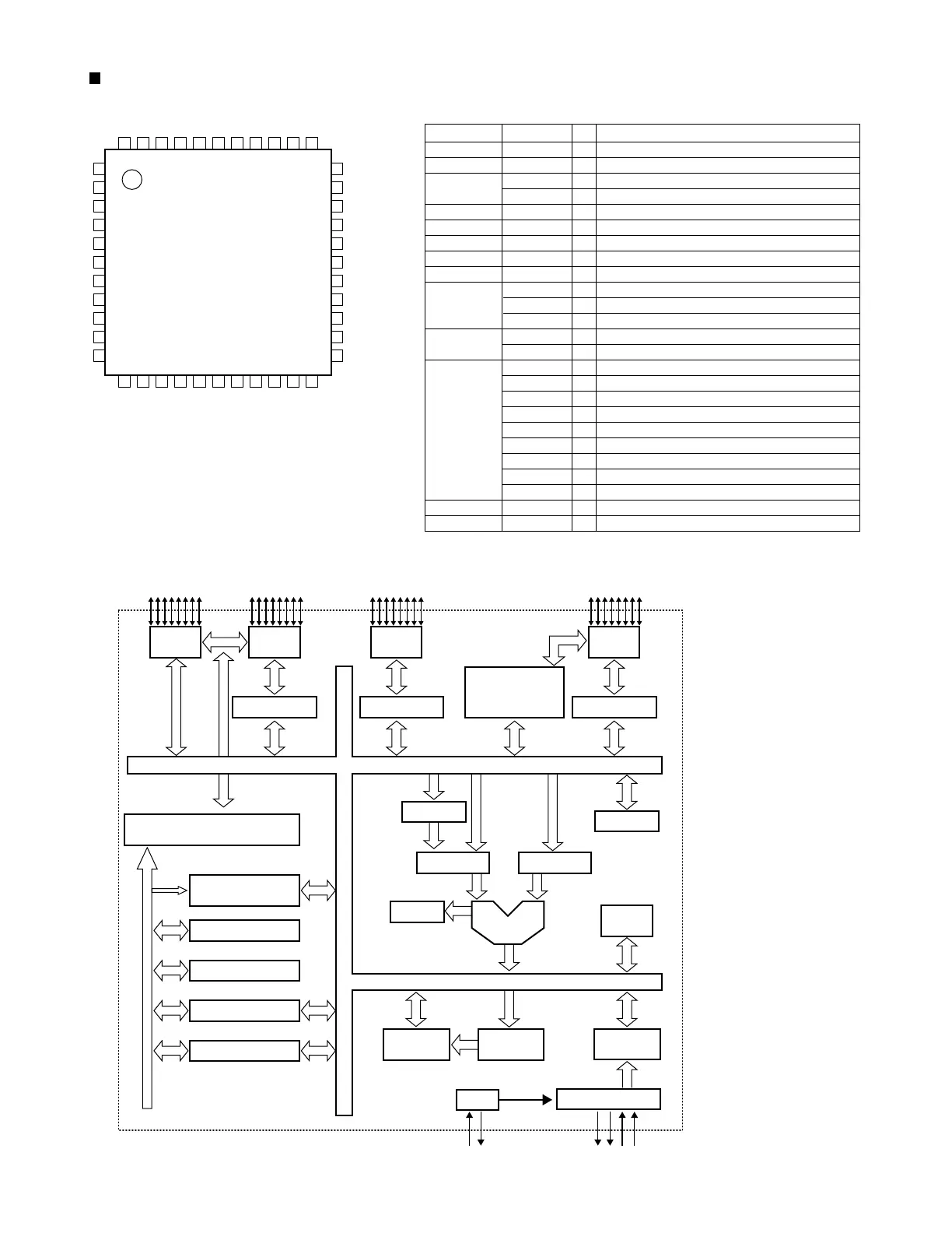
TH-A5R
1-27
M6759 (U3) : MTP microcontroller
3. Block diagram
1. Pin layout
1
2
3
4
5
6
7
8
9
10
11
33
32
31
30
29
28
27
26
25
24
23
44
43
42
41
40
39
38
37
36
35
34
12
13
14
15
16
17
18
19
20
21
22
P0.7:0 P2.7:0 P1.7:0 P3.7:0
RST
/EAVPP
ALE
/PSEN
XTAL2
XTAL1
Port 0
Drivers
Port 2
Drivers
Port 1
Drivers
Port 3
Drivers
Program Address
Register
Stack
Pointer
Instruction
Register
RAM Addr.
Register
512 Bytes
RAM
Port Latch
PSW
B Register
ACC
ALU REG1 ALU REG2
Clock and Control
OSC
Port Latch Port Latch
Serial Port
Timer
Interrupt Logic
ALU
64K bytes
MTP Memory
DPTR
Buffer
Incrementer
Program Counter
Data Bus
Data Bus
Data Bus
Data Bus
2. Pin function
Symbol
VDD
GND
P0.7-P0.0
AD7-0
RST
XTAL1
XTAL2
/PSEN
ALE
P1.7-P1.0
T2EX(P1.1)
T2(P1.0)
P2.7
A15-A8
P3.7-P3.0
/RD(P3.7)
/WR(P3.6)
T1(P3.5)
T0(P3.4)
/INT1(P3.3)
/INT0(P3.2)
TXD(P3.1)
RXD(P3.0)
/EAVPP
NC
Pin No.
44
22
36,37,38,39,
40,41,42,43,
10
21
20
32
33
9,8,7,6,
5,4,3,2
31,30,29,28,
27,26,25,24
19,18,17,16,
15,14,13,11
35
1,12,23,34
I/O
I
I
I/O
I/O
I
I
O
O
O
I/O
I
I
I/O
O
I/O
O
O
I
I
I
I
O
I
I
-
Description
Power supply for internal operation, 5V input
Ground
8 bits bi-directional I/O port
Multiplexed address/data bus
Reset signal
Crystal In
Crystal out
Program Store Enable Output
Address Latch Enable
8 bits bi-directional I/O port
External timer/counter 2 trigger
External timer/counter 2.
8 bits bi-directional I/O port
8-bit bi-directional I/O port
External data memory read strobe
External data memory write strobe
External timer/counter 1
External timer/counter .
External interrupt 1 (Negative Edge Detect)
External interrupt 0 (Negative Edge Detect)
Serial port output
Serial port input
 Loading...