TH-A5R
1-28
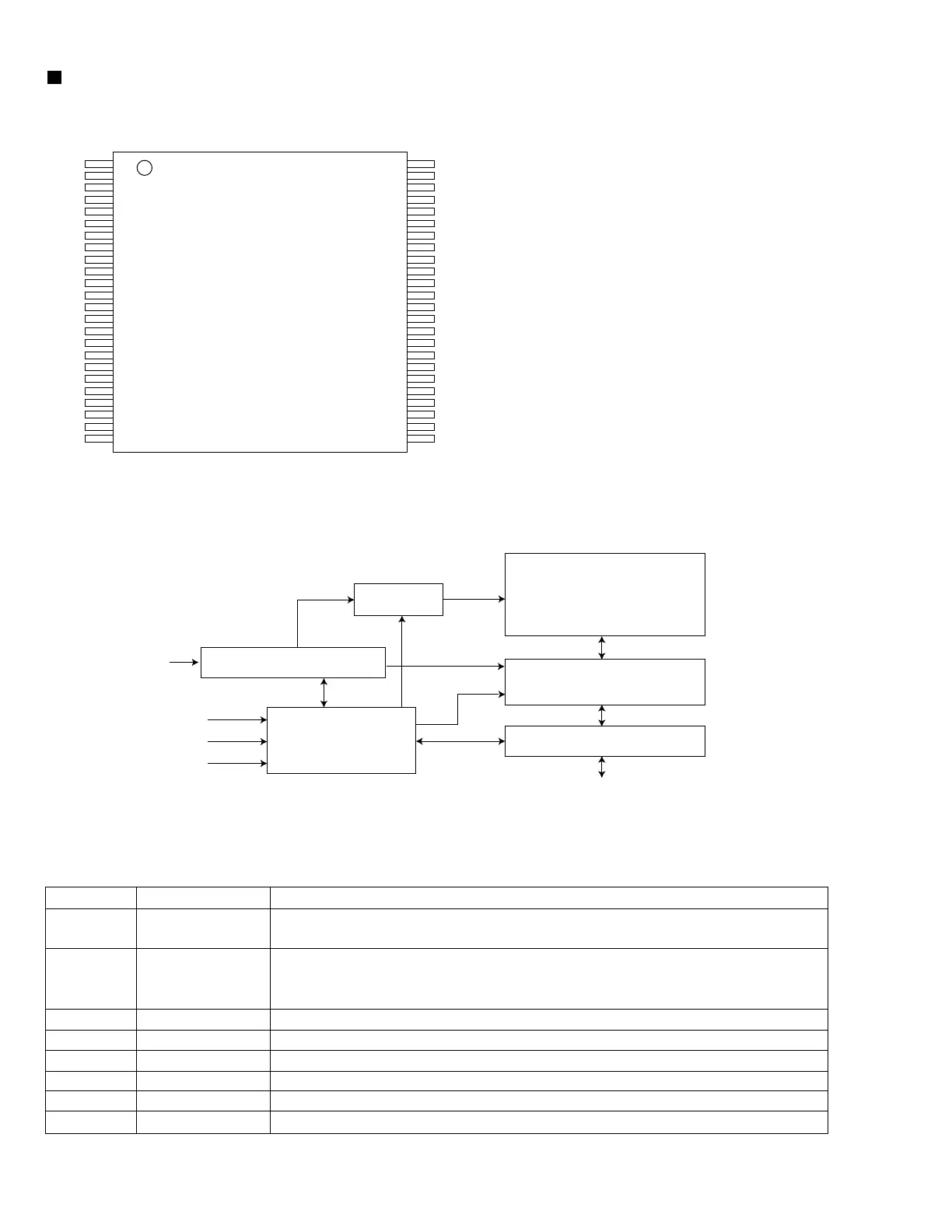
2. Block diagram
1. Pin layout
3. Pin function
X-Decoder
Address Buffer & Latches
Control Logic
Memory Address
CE#
OE#
WE#
EEPROM
Cell Array
Y-Decoder
I/O Buffers & Data Latches
DQ15-DQ0
1
2
3
4
5
6
7
8
9
10
11
12
13
14
15
16
17
18
19
20
21
22
23
24
48
47
46
45
44
43
42
41
40
39
38
37
36
35
34
33
32
31
30
29
28
27
26
25
A15
A14
A13
A12
A11
A10
A9
A8
NC
NC
WE#
NC
NC
NC
NC
A18
A17
A7
A6
A5
A4
A3
A2
A1
A16
NC
Vss
DQ15
DQ7
DQ14
DQ6
DQ13
DQ5
DQ12
DQ4
VDD
DQ11
DQ3
DQ10
DQ2
DQ9
DQ1
DQ8
DQ0
OE#
Vss
CE#
A0
Symbol
AMS- A0
DQ15- DQ0
CE#
OE#
WE#
VDD
Vss
NC
Pin name
Address Inputs
Data Input/Output
Chip Enable
Output Enable
Write Enable
Power Supply
Ground
No Connection
Function
To provide memory addresses. During Sector-Erase AMS-A11 address lines will
select the sector. During Block-Erase AMS-A15 address lines will select the block.
To output data during Read cycles and receive input data during Write cycles. Data is
internally latched during a Write cycle. The outputs are in tri-state when OE# or CE# is
high.
To activate the device when CE# is low.
To gate the data output buffers.
To control the Write operations.
To provide power supply voltage: 2.7-3.6V
Unconnected pins.
SST39VF800A (U6) : 8M Flash memory
 Loading...