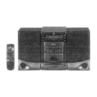
UX-A7DVD
(No.22013)1-51
4.11 K4S641632F-TC75 (IC504) :CMOS SDRAM
•Pin layout
• Block diagram
• Pin function
54 53 52 51 50 49 48 47 46 45 44 43 42 41 40 39 38 37
18 19 20 21 22 23 24 25 26 27
36 35 34 33 32 31 30 29 28
1716151413121110987654321
VDD
DQ0
VDDQ
DQ1
DQ2
VSSQ
DQ3
DQ4
VDDQ
DQ5
DQ6
VSSQ
DQ7
VDD
LDQM
WE
CAS
RAS
CS
BA0
BA1
DD
Data Input Register
1M
16
1M
16
1M
16
1M
16
Column Decoder
Latency & Burst Length
Programming Register
LDQMLWCBRLCASLWELCBRLRAS
DQ1
LWE
LDQM
Timing Register
Pin No. Symbol Function
1 VDD Power and ground for the input buffers and the core logic.
2 DQ0 Data inputs/outputs are multiplexed on the same pins.
3 VDDQ Isolated power supply and ground for the output buffers to provlde improved nolse immunity.
4 DQ1 Data inputs/outputs are multiplexed on the same pins.
5 DQ2 Data inputs/outputs are multiplexed on the same pins.
6 VSSQ Isolated power supply and ground for the output buffers to provlde improved nolse immunity.
7 DQ3 Data inputs/outputs are multiplexed on the same pins.
8 DQ4 Data inputs/outputs are multiplexed on the same pins.
 Loading...