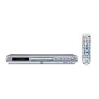
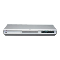
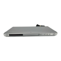
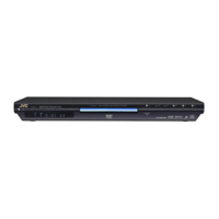
XV-N40BK,XV-N44SL
(No.A0040)1-29
4.6 JCE8045(IC501):AV Decoder
•Pin layout
• Block diagram
• Pin function
1
60
180
121
240 181
61 120
Pin No. Symbol I/O Description
1 VDDio - Power supply terminal 3.3V
2,3 MD10,11 I/O SDRAM Data bus terminal
4 VDD - Power supply terminal 1.8V
5 MD12 I/O SDRAM Data bus terminal
6 VSSio - Connect to ground
7~9 MD13~15 I/O SDRAM Data bus terminal
10 VDDio - Power supply terminal 3.3V
11 DQM1 O SDRAM Data byte enable
12,13 MA9,8 O SDRAM Address bus terminal
14 VSSio - Connect to ground
15,16 MA7,6 O SDRAM Address bus terminal
17 VSS - Connect to ground
18 MA5 O SDRAM Address bus terminal
19 VDDio - Power supply terminal 3.3V
20,21 MA4,3 O SDRAM Address bus terminal
22 MCLK O SDRAM Clock output
23 VSSio - Connect to ground
24 CKE O SDRAM Clock enable output
Audio
output
processor
Audio
DSP
MPEG
Video
decoder
Video
output
processor
NTSC
PAL
SCART
encoder
Serial
port
controller
XBUS
controller
DVD
A/V
+
CSS
Demux
engine
SDRAM
controller
RISC
uProcessor
+ cache
Video
XBUS
SDRAM
Video I/O port
audio DAC
digital audio
digital audio
serial
peripherals
DVD data
 Loading...