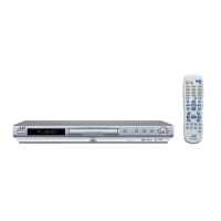
XV-N40BK,XV-N44SL
(No.A0040)1-39
4.9 PT6315-S(IC801):FL Display driver and key controller
•Pin layout
• Pin function
CLK
STB
K1
K2
VSS
VDD
SG1
SG2
SG3
SG4
SG5
SG6
SG7
SG8
DIN
DOUT
OSC
VSS
VDD
GR1
GR2
GR3
GR4
GR5
GR6
GR7
SG9
VEE
1
2
3
4
5
6
7
8
9
10
11
12
13
14
28
27
26
25
24
23
22
21
20
19
18
17
16
15
Pin No. Symbol I/O Description
1 CLK I Clock input terminal
2 STB I Serial interface strobe terminal
3,4 K1,K2 I Key data input terminal
5 VSS - Connect to ground
6 VDD - Power supply terminal
7~14 SG1~SG8 O FL Display segment control signal output terminal
15 VEE - Pull-down level
16 SG9 O FL Display segment control signal output terminal
17~23 GR7~GR1 O FL Display grid control signal output terminal
24 VDD - Power supply terminal
25 VSS - Connect to ground
26 OSC I Oscillator input terminal
27 DOUT O Data output terminal
28 DIN I Data input terminal
 Loading...