5
ECP5 PCI Express Board User’s Guide
Figure 4. ECP5 Configuration Pin (CFG pins)
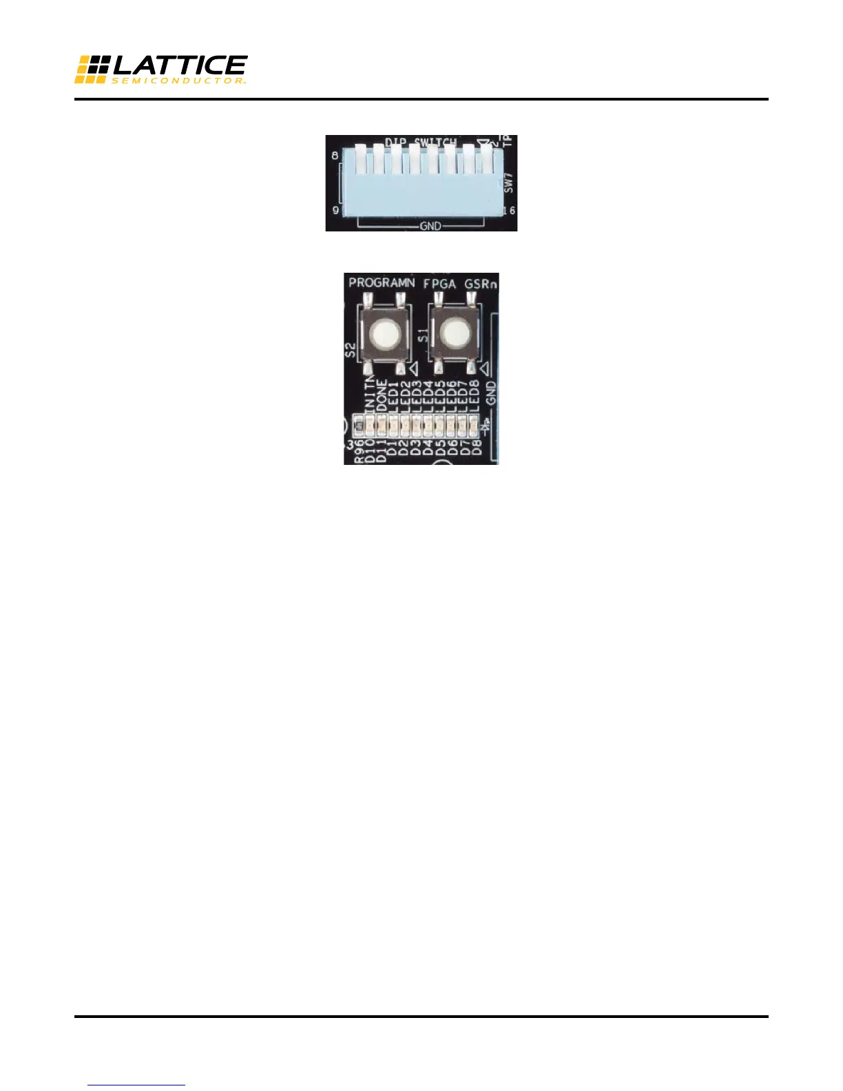
Figure 5. ECP5 Status LEDs and Push-button Controls
The LEDs indicate the configuration status of the ECP5 FPGA.
• D10 (red) illuminated indicates that programming was aborted or reinitialized, driving the INITN output low.
• D11 (green) illuminated indicates the successful completion of configuration by releasing the open collector
DONE output pin.
PROGRAMN and GSRN
These push-button switches assert/de-assert the logic levels on PROGRAMN (S2) and GSRN (S1). Depress- ing
the button drives a logic level “0” to the device.
Programming Serial SPI Flash Memory
A serial SPI (16-pin TSSOP, 128Mb) Flash memory device (U52) is on-board for non-volatile configuration memory
storage. A Micron N25Q128A device is populated on-board.
The Serial SPI Flash memory device can be configured easily via the ECP5 JTAG port. This mode enables the
FPGA to be programmed at power-up or assertion of PROGRAMN with a bitstream stored in the memory device.
1. Connect the ECP5 PCI Express Board.
2. Scan the board or select the ECP5UM-85F device.
3. From the Edit pull down menu select Device Properties. Set the Access mode to SPI Flash Background Pro-
gramming and Operation to SPI Flash Erase, Program, Verify.