8
ECP5 PCI Express Board User’s Guide
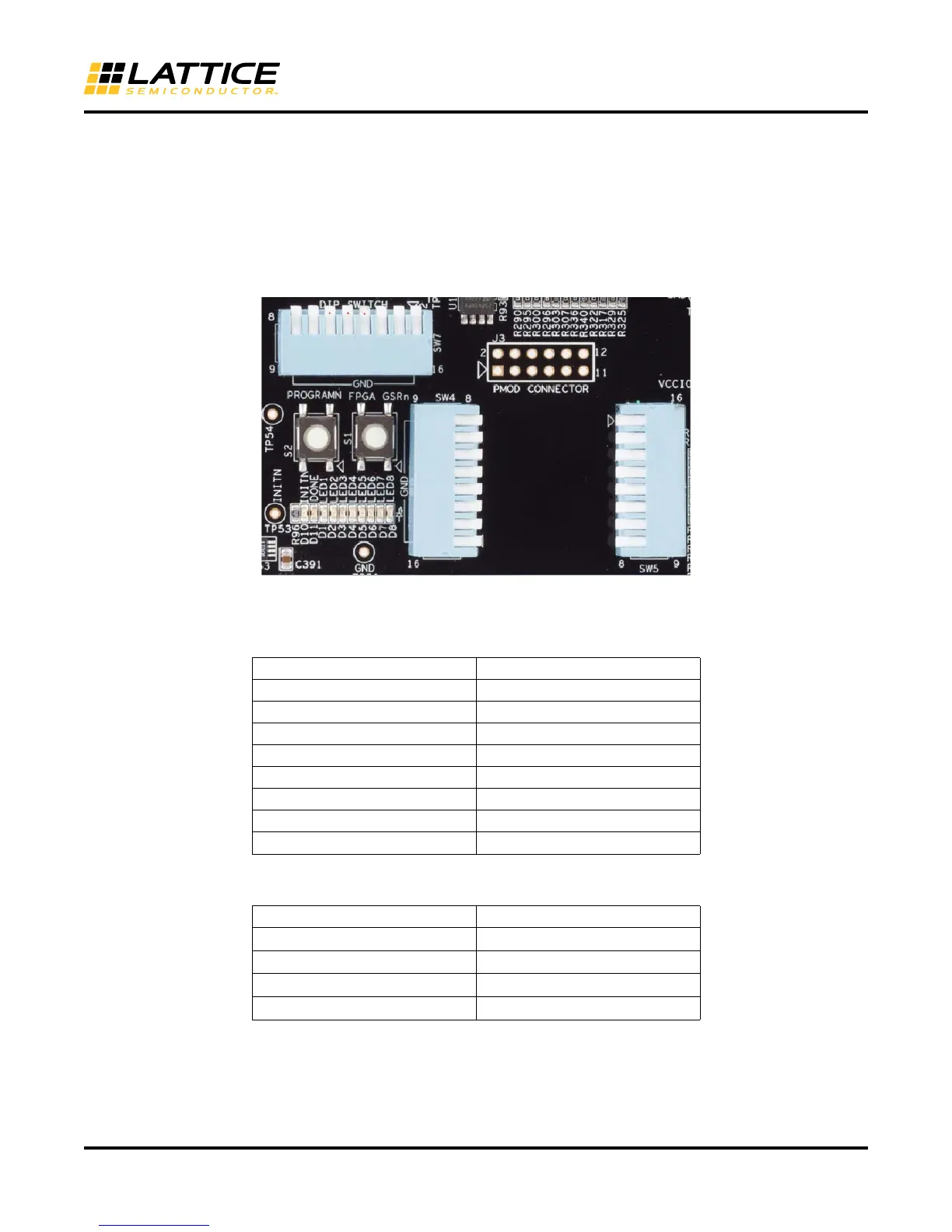
FPGA Test Pins (See Appendix B, "ECP5 Config" and "LEDs and Switches" sheets)
General Purpose DIP Switches
General purpose FPGA pins are available for user applications. FPGA pins are connected to switch SW4, SW7
with a piano style DIP switch. The switches are connected to logic level 0 when Down, logic level 1 when Up.
Switch position 1 is indicated with a dot. Switch SW4 logic 1 is 2.5V. Switch SW4 logic 1 is 2.5V. The user must pro-
gram these inputs to be the LVCMOS25 or LVCMOS33 type in the design.
Figure 8. ECP5 PCI Express Board LEDs and Switches
The designated pins are connected according to Table 5.
Table 3. FPGA Ball to DIP Switch Position
FPGA Ball Number SW4 DIP Switch Position
AK31 1
AM31 2
AJ31 3
AL32 4
AG28 5
AJ28 6
AG29 7
AH28 8
FPGA Ball Number SW7 DIP Switch
Position
F31 4
F32 5
E32 6