2-24
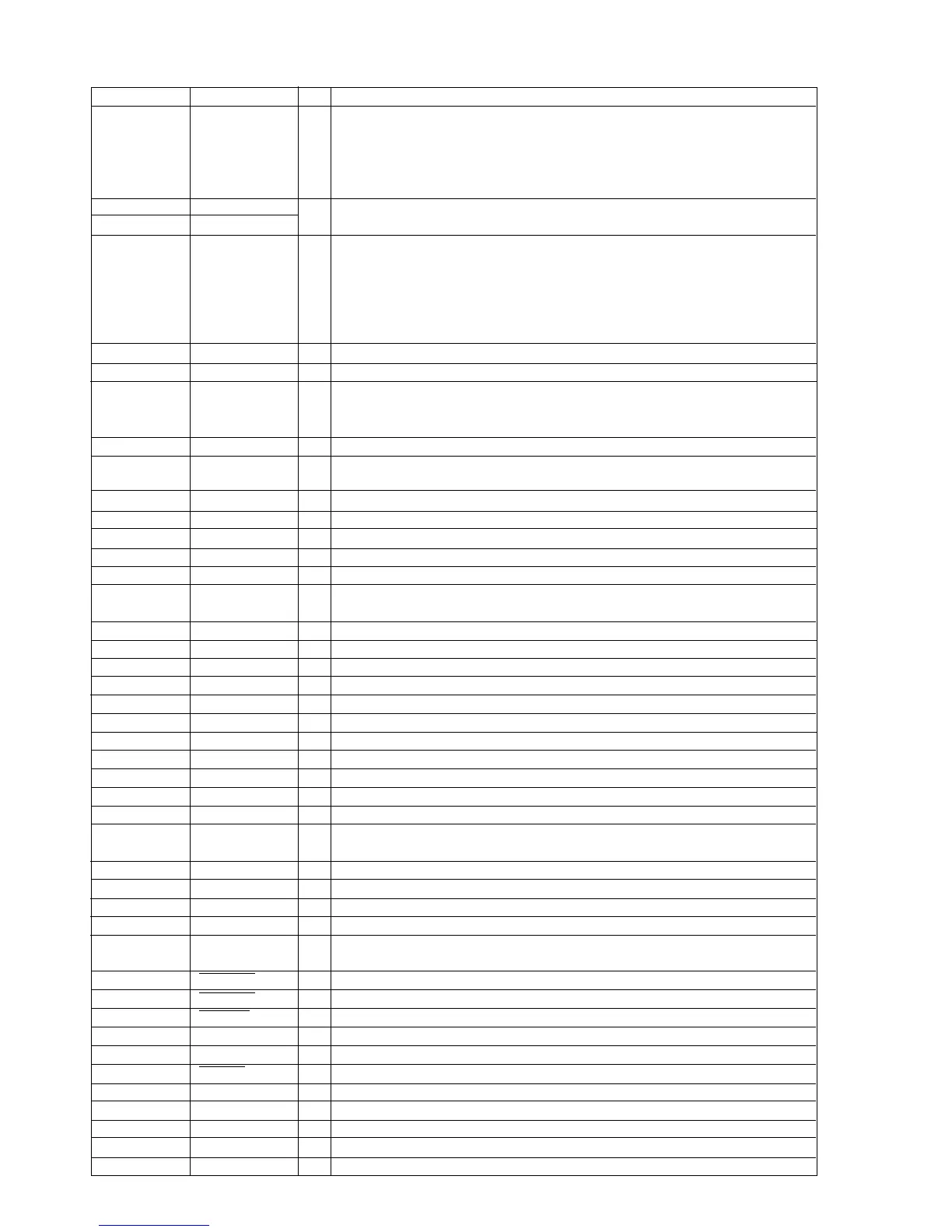
Pin No. Port Name I/O FUNCTION
1,12,26,35,46,
52,63,73,81,
95,105,118, VSS1-18 Ð Ground pins.
131,142,156,
170,182,195
2 SEL0
Ð Test mode select pins.
3 SEL1
4-6,8,10,10
11,14-22,28
29,116,117
119,125,126 TEST9-46 Ð Test mode output pins. (Leave them open)
132,171-174
194,197-206
7 AVRTM O End of output stream of 2060 bytes data to CSS.
9 XSRTM O End of block signal.
13,25,33,45,53,
62,72,140,157, VDD5-1to 5-12 Ð +5 V power supply pin.
169,196,208
23 MLD O Microprocessor command load signal for CD-DA section. (L: load).
24 MCLK O
Microprocessor command clock signal for CD-DA section.
(data is atched on rising edge)
25 VDD5-2 Ð +5 V power supply pin.
26 VSS3 Ð Ground pin.
27 MDATA O Microprocessor command data for CD-DA section.
30 DEMPH I De-emphasis control input (H: on).
31 DMUTE O Muting output for CD-DA section.
32 STAT I
Status signal (CRC, CUE, CLVS, TTSTOP, FCLV, SQOK) from CD-DA, STAT
also goes to CPU.
34 PLLCLK I 27 MHz clock input pin.
36 CHNDATA I Inverted bit data, which is changed on the falling edge of PLLCLK.
37 SDTIO I/O Serial bit data I/O.
38 ASPSCK O 296ns clock (27 MHz/8) output.
39 SEN O High enable CPU to write data to 8 read-channel registers.
40 PLLOK O DVD frame sync (H: O.K)
41 LDON O Turn on the Laser diode.
42 XDVD O DVD mode control output.
43 XCD2 O 2X CD mode control output.
44 XCD4 O 4X CD mode control output.
47-51,54-56 SRMDT0-7 I/O SRAM data bus.
57-61,64-71
SRMADR0-16 O SRAM address bus.
74-77
78 XSRMCE O Chip enable signal to SRAM.
79 XSRMOE O Output enable signal to SRAM.
80 XSRMWE O Write enable signal to SRAM.
83-90 SDMDT0-7 I/O SDRAM data bus.
91-93
SDMADR0-11 O SDRAM address bus.
96-103,106
107 SDMRAS O SDRAM row address strobe output.
108 SDMCAS O SDRAM column address strobe output.
109 SDMWE O SDRAM write enable output.
110 SDMDQML O SDRAM lower byte input/output mask.
111 SDMCLK O Clock signal output to SDRAM.
112 SDMCS O SDRAM chip select control.
113 SDMDQML O SDRAM upper byte input/output mask.
115 SDMCKE O SDRAM clock enable.
120 XDSCO O Chip select signal to the SERVO MI-COM.
121 CRCOK O Sector IDs are O.K.
122-124 CPUADR0-2 O (Video/Audio) HAL [2:0], V/A decoder, CPU address bus.
YMC13D000 (DVD Sync/ECC/Formatter)
 Loading...