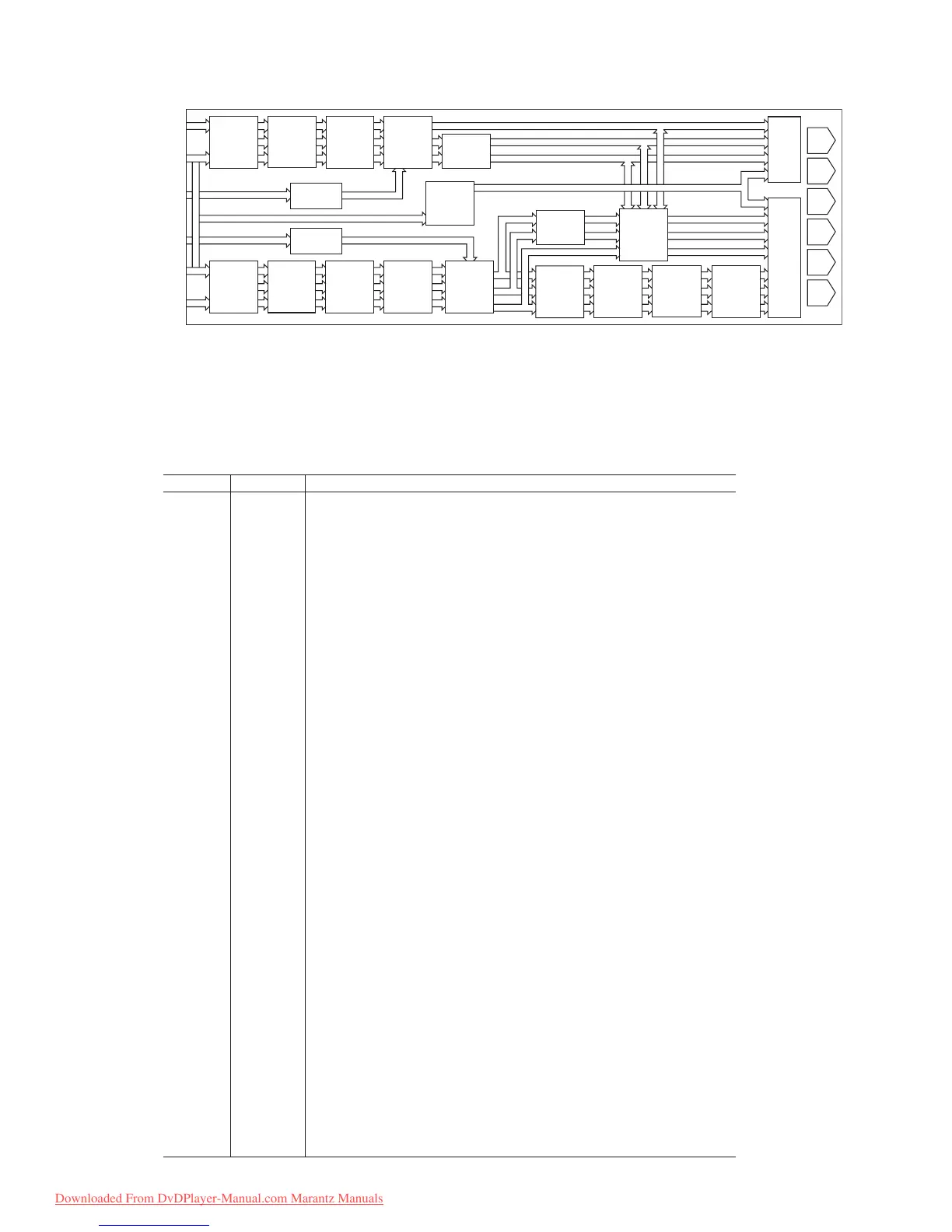
_VSYNC
CLKIN_B
HD PIXEL
INPUT
SD PIXEL
INPUT
DE-
INTER-
LEAVE
Y
CB
CR
TEST
PATTERN
SHARPNESS
AND
ADAPTIVE
FILTER
CONT
LUMA
AND
CHROMA
FILTERS
ROL
Y COLOR
CR COLOR
CB COLOR
4:2:2
TO
4:4:4
TIMING
GENERATOR
TIMING
GENERATOR
DE-
INTER-
LEAVE
Y
CB
CR
TEST
PATTERN
DNR
GAMMA
COLOR
CONTROL
SYNC
INSERTION
CLOCK
CONTROL
AND PLL
UV SSAF
V
U
PS 8
HDTV 2
RGB
MATRIX
SD 16
2 OVER-
SAMPLING
DAC
DAC
DAC
DAC
DAC
DAC
F
SC
MODULATION
CGMS
WSS
TERMINOLOGY
SD Standard Definition Video, conforming to
ITU-R BT.601/ITU-R BT.656.
HD High Definition Video, i.e., Progressive Scan or HDTV.
PS Progressive Scan Video, conforming to SMPTE 293M,
ITU-R BT.1358, BTAT-1004EDTV2, or BTA1362.
HDTV High Definition Television Video, conforming to
SMPTE 274M or SMPTE 296M.
YCrCb SD, PS, or HD Component Digital Video.
YPrPb SD, PS, or HD Component Analog Video.
Mnemonic Input/Output Function
DGND G Digital Ground.
AGND G Analog Ground.
CLKIN_A I Pixel Clock Input for HD (74.25 MHz Only, PS Only (27 MHz), SD Only (27 MHz).
CLKIN_B I Pixel Clock Input. Requires a 27 MHz reference clock for progressive scan mode or a 74.25 MHz
(74.1758 MHz) reference clock in HDTV mode. This clock is only used in dual modes.
COMP1,2 O Compensation Pin for DACs. Connect 0.1 F capacitor from COMP pin to V
AA
.
DAC A O CVBS/Green/Y/Y Analog Output.
DAC B O Chroma/Blue/U/Pb Analog Output.
DAC C O Luma/Red/V/Pr Analog Output.
DAC D O In SD Only Mode: CVBS/Green/Y Analog Output; in HD Only Mode and Simultaneous HD/SD
Mode: Y/Green [HD] Analog Output.
DAC E O In SD Only Mode: Luma/Blue/U Analog Output; in HD Only Mode and Simultaneous HD/SD
Mode: Pr/Red Analog Output.
DAC F O In SD Only Mode: Chroma/Red/V Analog Output; in HD Only Mode and Simultaneous HD/SD
Mode: Pb/Blue [HD] Analog Output.
P_HSYNC I Video Horizontal Sync Control Signal for HD in Simultaneous SD/HD Mode and HD Only Mode.
P_VSYNC I Video Vertical Sync Control Signal for HD in Simultaneous SD/HD Mode and HD Only Mode.
P_BLANK I Video Blanking Control Signal for HD in Simultaneous SD/HD Mode and HD Only Mode.
S_BLANK I/O Video Blanking Control Signal for SD Only.
S_HSYNC I/O Video Horizontal Sync Control Signal for SD Only.
S_VSYNC I/O Video Vertical Sync Control Signal for SD Only.
Y9–Y0 I SD or Progressive Scan/HDTV Input Port for Y Data. Input port for interleaved progressive scan
data. The LSB is set up on Pin Y0. For 8-bit data input, LSB is set up on Y2.
C9–C0 I Progressive Scan/HDTV Input Port 4:4:4 Input Mode. This port is used for the Cb[Blue/U] data.
The LSB is set up on pin C0. For 8-bit data input, LSB is set up on C2.
S9–S0 I SD or Progressive Scan/HDTV Input Port for Cr[Red/V] data in 4:4:4 input mode. LSB is set up
on pin S0. For 8-bit data input, LSB is set up on S2.
RESET I This input resets the on-chip timing generator and sets the ADV7310/ADV7311 into default register
setting. RESET is an active low signal.
R
SET1,2
I A 3040 Ω resistor must be connected from this pin to AGND and is used to control the amplitudes
of the DAC outputs.
SCLK I I
2
C Port Serial Interface Clock Input.
SDA I/O I
2
C Port Serial Data Input/Output.
ALSB I TTL Address Input. This signal sets up the LSB of the I
2
C address. When this pin is tied low,
the I
2
C filter is activated, which reduces noise on the I
2
C interface.
V
DD_IO
P Power Supply for Digital Inputs and Outputs.
V
DD
P Digital Power Supply.
V
AA
P Analog Power Supply.
V
REF
I/O Optional External Voltage Reference Input for DACs or Voltage Reference Output (1.235 V).
EXT_LF I External Loop Filter for the Internal PLL.
RTC_SCR_TR I Multifunctional Input. Real time control (RTC) input, timing reset input, subcarrier reset input.
I
2
C I This input pin must be tied high (V
DD_IO
) for the ADV7310/ADV7311 to interface over the I
2
C port.
GND_IO Digital Input/Output Ground.
Downloaded From DvDPlayer-Manual.com Marantz Manuals