HCS300
DS21137G-page 22 © 2011 Microchip Technology Inc.
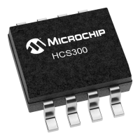
FIGURE 9-1: POWER-UP AND TRANSMIT TIMING
TABLE 9-3: POWER-UP AND TRANSMIT TIMING
(2)
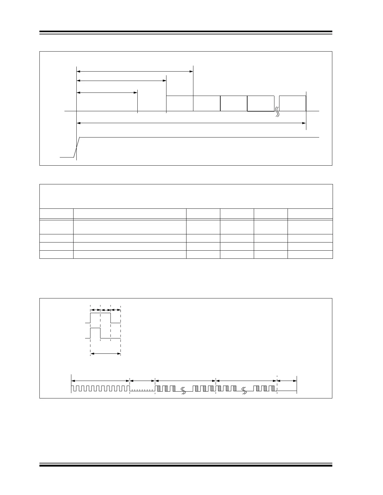
FIGURE 9-2: CODE WORD FORMAT
VDD = +3.5 to 13.0V
Commercial(C): Tamb = 0°C to +70°C
Industrial(I): Tamb = -40°C to +85°C
Symbol Parameter Min Max Unit Remarks
TBP Time to second button press 10 + Code
Word
26 + Code
Word
ms (Note 1)
T
TD Transmit delay from button detect 10 26 ms
TDB Debounce Delay 6 15 ms
T
TO Auto-shutoff time-out period 20 120 s
Note 1: T
BP is the time in which a second button can be pressed without completion of the first code word and the
intention was to press the combination of buttons.
2: Typical values - not tested in production.
Button Press
Sn
Detect
T
DB
Output
TTD
Multiple Code Word Transmission
TTO
Code
Word
1
Code
Word
2
Code
Word
3
Code
Word
n
T
BP
Code
Word
4
PWM
Input
Button
LOGIC ‘0’
LOGIC ‘1’
Bit Period
Preamble
Header
Encrypted Portion
of Transmission
Fixed Portion of
Transmission
Guard
Time
TP
TH
THOP
TFIX
TG
50% Duty Cycle
T
BP
TE
TE
TE