Receiver 2-3
3.0 Receiver
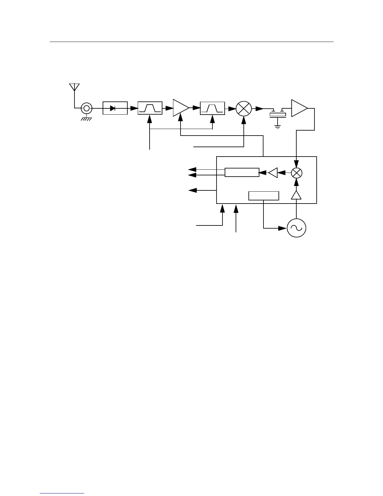
3.1 Receiver Front-End
(Refer to Figure 2-2 and the Receiver Front End schematic diagram)
The RF signal is received by the antenna and applied to a low-pass filter. For 300R1, the filter
consists of L101, L102, C102, C103, C104. The filtered RF signal is passed through the antenna
switch. The antenna switch circuit consists of two PIN diodes (CR101 and CR102) and a pi network
(C106, L104 and C107). The signal is then applied to a varactor tuned bandpass filter. The VHF
bandpass filter comprises of L301, L302, C302, C303, C304, CR301 and CR302. The bandpass
filter is tuned by applying a control voltage to the varactor diodes (CR301 and CR302) in the filter.
The bandpass filter is electronically tuned by the DACRx from U404 which is controlled by the
microprocessor. Depending on the carrier frequency, the DACRx will supply the tuned voltage to the
varactor diodes in the filter. Wideband operation of the filter is achieved by shifting the bandpass
filter across the band.
The output of the bandpass filter is coupled to the RF amplifier transistor Q301 via C307. After being
amplified by the RF amplifier, the RF signal is further filtered by a second varactor tuned bandpass
filter, consisting of L306, L307, C313, C317, CR304 and CR305.
Figure 2-2 Receiver Block Diagram
Demodulator
Synthesizer
Crystal
Filter
Mixer
Varactor
Tuned Filter
RF Amp
Varactor
Tuned Filter
Pin Diode
Antenna
Switch
RF Jack
Antenna
AGC
Control Voltage
from ASFIC
First LO
from FGU
Recovered Audio
Squelch
RSSI
IF
IC
SPI Bus
16.8 MHz
Reference Clock
Second
LO VCO
U301
IF Amp

 Loading...