Do you have a question about the Motorola MVME147 and is the answer not in the manual?
Provides an overview of the manual's content for the MVME147 series of MPU VMEmodules.
Lists the available MVME147 models and notes differences in memory maps.
Details the features of the MVME147, including microprocessor, memory, I/O, and interfaces.
Lists general specifications, cooling requirements, and FCC compliance for the MVME147.
Describes the operating temperature range and cooling methods for reliable operation.
Outlines the conditions met for FCC compliance for Class A equipment.
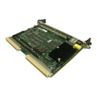
Provides a detailed description of the MVME147 module based on the MC68030 microprocessor.
Lists the essential equipment needed to set up and operate the MVME147 system.
Lists supplementary publications that provide additional helpful information about the MVME147.
Outlines the chapter's content: unpacking, hardware preparation, and installation instructions.
Provides steps for safely unpacking the MVME147 module and its components.
Lists essential steps for using the board and refers to relevant sections for detailed information.
Explains factory-tested jumper configurations and how to modify them for desired system functions.
Details how to configure ROM/PROM/EPROM/EEPROM sockets using J1 and J2 headers.
Provides step-by-step instructions for installing the MVME147 module into a chassis.
Introduces the chapter on using the MVME147 in a system configuration.
Describes the front panel switches (ABORT, RESET) and LED status indicators (FAIL, STATUS, RUN, SCON).
Explains the function of the front panel RESET switch, including local and VMEbus reset.
Details the FAIL LED's indication of BRDFAIL status or watchdog time-out.
Explains the STATUS LED indicates the MC68030 STATUS* pin state.
Describes the RUN LED indicating MC68030 address strobe activity.
Explains the SCON LED indicates the MVME147's role as VMEbus system controller.
Introduces memory mapping perspectives: MC68030 and VMEbus views.
Explains how the MC68030 memory map is split by function codes and device responses.
Details the main memory map, including address ranges, devices accessed, port size, and cache inhibit.
Lists local I/O devices with their address ranges, port size, and notes.
Describes CPU space cycles for coprocessor and interrupt acknowledge.
Describes MVME147 resources as viewed by VMEbus masters.
Table showing DRAM address ranges and their mapping from the VMEbus perspective.
Describes the VMEchip GCSR appearing at odd addresses in the VMEbus short I/O map.
Table mapping VMEchip GCSR register bits to short I/O addresses.
Introduces the chapter on programming the Peripheral Channel Controller (PCC) and VMEchip.
Details PCC internal registers, bit assignments, and their operations.
Provides an overview of PCC registers, including 32-bit, 16-bit, and 8-bit register definitions.
Describes the Timer 1 Control Register for timer enable, stop, and overflow counter functions.
Describes the Watchdog Timer Control Register for enabling the timer and setting time-out limits.
Describes the DMA Control and Status Register for enabling the controller and defining transfer modes.
Describes the Slave Base Address Register for setting onboard RAM base address.
Details the VMEchip registers, including Local Control and Status Registers (LCSR).
Describes the System Controller Configuration Register for VMEbus arbitration and SYSFAIL* signals.
Describes the Master Configuration Register for VMEbus data transfer capabilities and address modifiers.
Details the Timer Configuration Register for local and VMEbus access time-out periods.
Describes the Slave Address Modifier Register for configuring VMEbus master access to onboard DRAM.
Describes the Master Address Modifier Register for programming VMEbus address modifier codes.
Details the Interrupt Handler Mask Register for enabling MC68030 response to VMEbus interrupt requests.
Introduces the chapter on functional description, providing an overview and block diagram.
Lists the components of the MVME147 as a complete microcomputer system.
Describes the MC68030 as the main processor, its caches, and cache inhibit function.
Describes the VMEchip ASIC for VMEbus interfacing, listing its functions.
Illustrates the functional blocks of the MVME147 and their interconnections.
Details the VMEbus system controller function provided by the VMEchip.
Describes the GCC ASIC, its features, and its role in replacing PALs and other devices.
Describes the PCC ASIC, listing its features like DMA, SCSI interface, and timers.
Describes onboard DRAM accessibility, parity features, and selectable parity modes.
Lists the five sources of reset for the MVME147, including SYSRESET*, power-on, and watchdog.
Describes conditions causing local bus errors, VMEbus access time-outs, and VMEbus BERR*.
Explains MVME147 support for indivisible Single Address (SARMC) and Multiple Address (MARMC) cycles.
Introduces the EIA-232-D standard, its applications, and the importance of following the standard.
Table listing standard EIA-232-D pin numbers, mnemonics, and signal descriptions.
Discusses the use of ground pins (SIGNAL GROUND, CHASSIS GROUND) and potential issues.
Provides an overview of the M68000 firmware family and its implementation on MVME147.
Describes 147Bug as a powerful evaluation and debugging tool for the MVME147.
Details 147Bug's physical storage in EPROMs, assembler code usage, and checksumming.
Describes the Autoboot routine for independent operating system booting and its configuration.
Explains the ROMboot function, its requirements, and preparation steps using the Checksum command.
Explains how to initialize the system to a known state using different reset modes.
Describes COLD and WARM reset modes, their effects on the system and debugger environment.
Explains how to invoke the ABORT switch, its effect on processor state, and interrupt generation.
Details the memory requirements for 147Bug operation and user space.
Describes 147Bug's disk I/O capabilities, including command-level operations and system calls.
Describes MVME147 dual-port RAM feature for shared access and remote processor control.
Lists hardware diagnostics for testing and troubleshooting the MVME147.
Explains how to use the 147Bug debugger, including entering commands and using syntactic variables.
Describes address parameter formats accepted by 147Bug, including register indirect modes.
Describes methods to enter user programs for execution using MM, download, or disk commands.
Explains how to avoid contaminating the debugger's operating environment and resource usage.
Describes MMU support in 147Bug, including confidence checks, commands, and data types.
Summarizes 147Bug debugger commands and explains symbols used in syntax.
Explains initial setup required for MVME147 operation, including setting time/date and verifying parameters.
Describes the interactive dialog for setting the date, time, and calibration values.
Describes the ENV command for selecting the debugger execution environment.
Explains how to use ENV with the D option to update NVRAM with default environmental parameters.
Describes the interactive prompts for selecting Bug Mode or System Mode when using ENV without options.
Lists seven VMEchip options available through ENV and describes Board ID and GCSR offset.
Provides basic steps to troubleshoot issues like no display, incorrect jumper settings, or terminal configuration.
Covers troubleshooting for keyboard input issues and problems preventing the debug prompt or auto-boot.
Addresses issues where the debug prompt appears but the board doesn't auto-boot, suggesting environment parameter checks.
Troubleshooting for NVRAM corruption, including initializing NVRAM and assigning Ethernet address.
Covers scenarios where the debugger is in System Mode or the board has passed self-tests, and issues with failed tests.
| Processor | Motorola 68030 |
|---|---|
| Clock Speed | 25 MHz |
| Bus Type | VMEbus |
| Ethernet | 10Base-T |
| Real-Time Clock | Yes |
| VMEbus Interface | A32/D32, A24/D16 |
| Operating System | VxWorks, OS-9 |
| Power Supply | +5V |
| Form Factor | 6U |
| I/O Interfaces | Typically includes SCSI, parallel port |
| Serial Ports | Two RS-232 serial ports |