Do you have a question about the MSI ms-7377 and is the answer not in the manual?
| Brand | MSI |
|---|---|
| Model | ms-7377 |
| Category | Motherboard |
| Language | English |
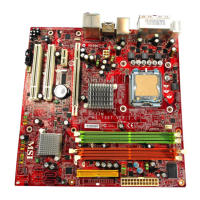
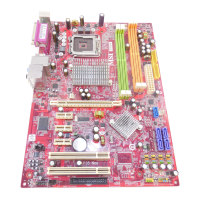
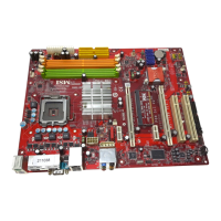
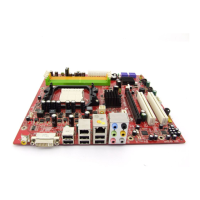
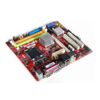
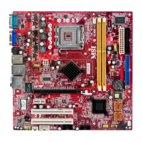
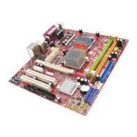
Overview of the motherboard's functional blocks and interconnections.
Detailed pinout and signal connections for the Intel LGA775 processor.
Power supply connections and VTT termination for the CPU.
Ground connections for the Intel LGA775 processor.
Functional overview of the Bearlake chipset components.
Signal connections for FSB, PCIE, and DMI interfaces.
Pin assignments and signals for DDR2 memory modules.
Termination resistors and decoupling capacitors for DDR2 memory.
Summary of power requirements for Bearlake chipset and related components.
Detailed ground pin assignments for the Bearlake chipset.
Signal connections for the ICH9's PCI interface.
Signal connections for the ICH9's USB ports.
Signal connections for the ICH9's Direct Media Interface.
Signal connections for the ICH9's PCI Express interface.
Host interface signals for the ICH9.
Signal connections for the ICH9's SATA ports.
SPI interface signals for the ICH9.
Audio interface signals managed by the ICH9.
Real-Time Clock and MSIC signals for ICH9.
Power requirements for the ICH9 chipset.
Pin assignments for DDR2 DIMM slots A1 and A2.
Pin assignments for DDR2 DIMM slots B1 and B2.
Termination resistors and decoupling capacitors for DDR2 memory.
Pin configuration for the CY505YC56DT clock generator chip.
Options for selecting CPU frequencies via jumpers and settings.
Pin assignments and functions of the IT8718F Super I/O controller.
Connections for FWH, Keyboard, and Mouse interfaces.
Details of SATA port connections and signals.
Serial communication port connections and signals.
Parallel printer port connections and signals.
Connections and configuration for the TPM security chip.
Signal assignments for the PCI Express x16 slot.
Signal assignments for the PCI Express x4 slot.
Pin configuration for the PCI slot (Ver: 2.3).
Resistor and capacitor placement for PCI slot signal integrity.
Power supply circuitry for USB ports, including ESD protection.
Wiring and connections for front-mounted USB ports.
Wiring and connections for rear-mounted USB ports.
Pinout and signal routing for the VGA connector.
Notes on component selection for specific VGA configurations.
Schematic of the VRD11 Intersil 6312 3-phase voltage regulator.
Guidelines for placing VRM components for optimal performance.
Pin assignments and functions of the MS7 ACPI controller.
Control signals for DDR VTT power management by ACPI.
Power management functions related to 1.5V rails.
Power supply circuit for the 3.3V CL rail.
Power supply circuit for the 1.25V CL rail.
Power supply circuit for the GMCH at 1.25V.
Circuit for selecting Front Side Bus voltage.
Control logic for the System Management (SLP_M) signal.
Wiring for front panel buttons, LEDs, and connectors.
Pinout and power signals for the ATX power supply connector.
Connections for CPU and System fan headers.
Pin assignments for the RJ45 LAN connector.
Detailed signal routing for the LAN controller.
Pin assignments for the Realtek ALC888 audio codec.
Connections for audio jacks and internal headers.
List of manual components and their part numbers.
Circuit for bleeding off residual voltage from power rails.
Configuration of ICH9 General Purpose Input/Output pins.
Configuration options via jumpers for system settings.
Configuration of the SIO 83627DHG controller.
Overview of power distribution to various motherboard components.
Diagram illustrating the Power OK signal path.
Diagram showing the reset signal path across components.
Log of changes and updates made to the document.