PAMS
Technical Documentation
NSE–3
Disassembly & Troubleshooting Instructions
Page 25
Original, 11/97
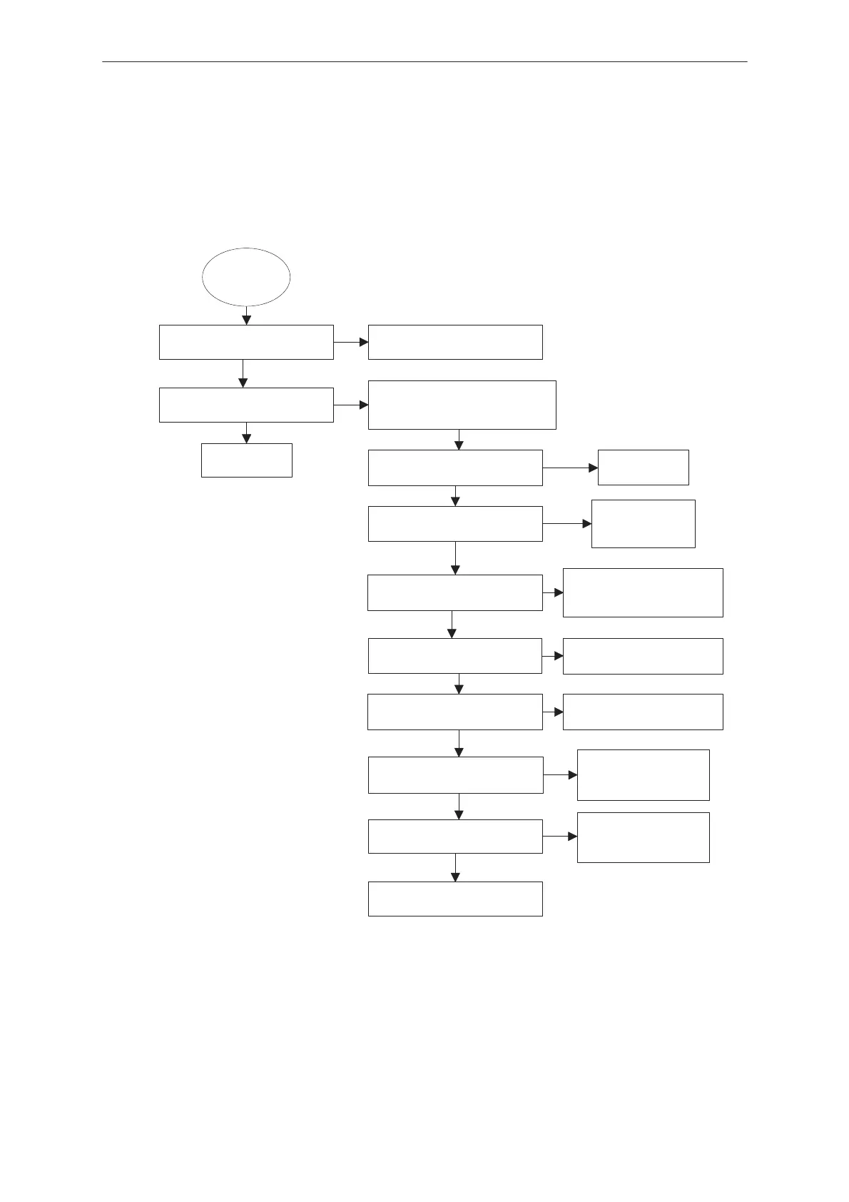
Receiver Fault (5)
UHFLO
G530 VCC–pin voltage, 2.8V
Check VSYN_1–line and R530
G530 VC(J500) voltage
~2.25V (Mid CH)
Check soldered joints
at G530, N620 and components
in VC–line
Does G530 oscillate at
any frequency
Change G530
N620 pin 21, 13 MHz clock
Check C633 and
soldering joints at
N620
N620 pin 9,22 and 25,
2.8V
Check VSYN_2(J508)
from CCONT and
CNTVR3–control from MAD
Check VCP–voltage
from CCONT pin 32
N620 pin 58,
1.5V
Check VREF_1–line
N620 pin 59,
loading 15 k
Ω
Check soldering joints
at N620 and R635, if
OK change R635
SCLK, SDATA, SENA1
working OK
Check SCLK, SDATA,
SENA1–lines from
MAD
Change N620
YES
YES
YES
YES
Change G530
YES
YES
YES
YES
N620 17 and 28,
5V
YES
NO
NO
NO
NO
NO
NO
NO
NO
NO
13 MHz clock oscilloscope picture in Appendix A
SCLK, SDATA, SENA1 oscilloscope pictures in Appendix B
YES
 Loading...