PAMS
Technical Documentation
NSE–3
Disassembly & Troubleshooting Instructions
Page 29
Original, 11/97
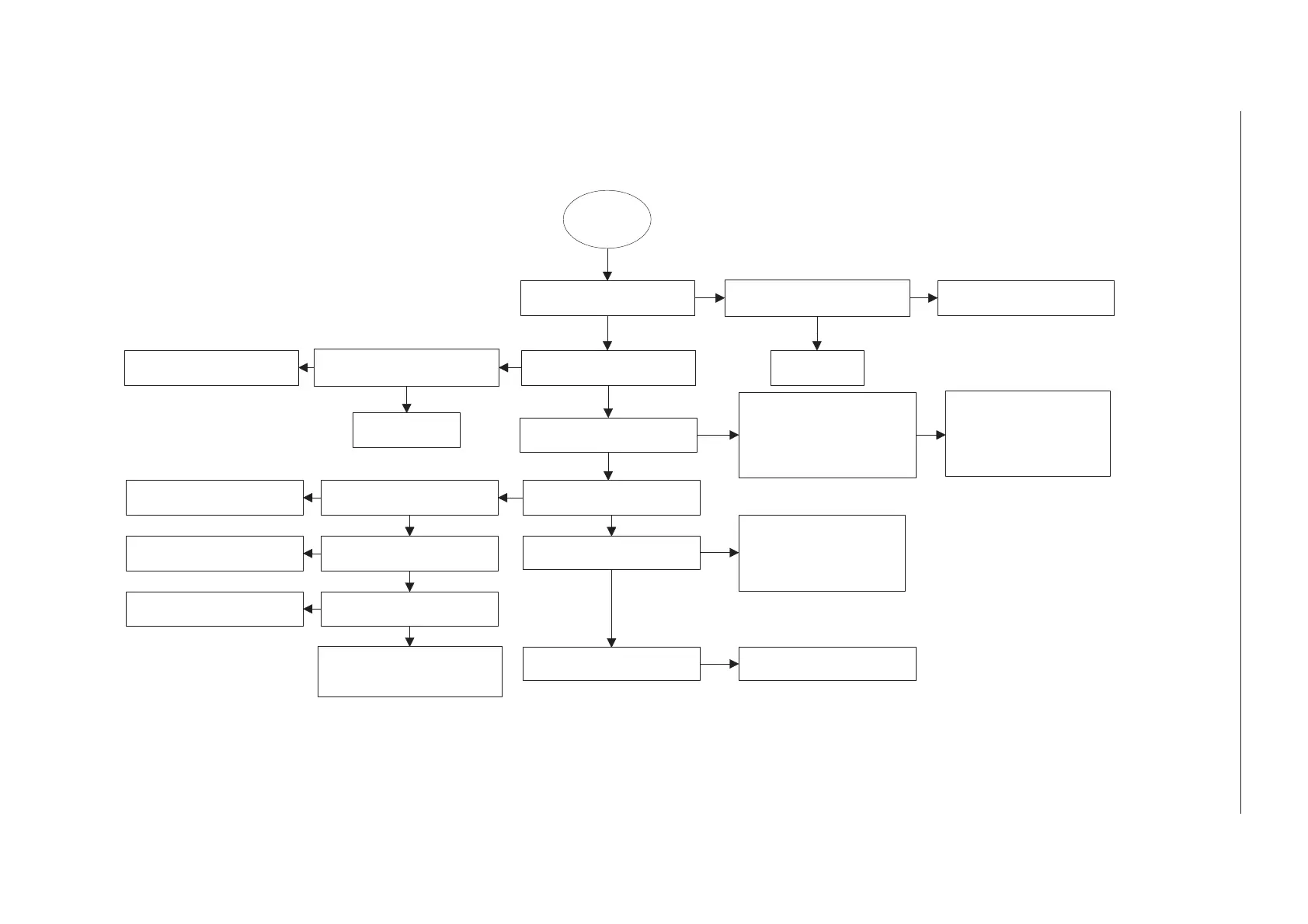
Transmitter Fault (2)
Transmitter
1
TXLEV5
Z505 input,
SL: – 23 dBm
Z505 input,
loading > 1 M
Ω
Check Z505 input for short
circuits, if OK change Z505
Check C700
Z505 output,
SL: –29 dBm
Z505 output,
loading > 1 M
Ω
Check Z505 output for short
circuits, if OK change Z505
Change Z505
N550 pin 8,
SL: –29 dBm
Check V640 limiter circuit
DC–levels(VTX–voltage),
Base: ~0.6V
Collector: ~0.6V
Emitter: ~0.3V
N550 pin 13,
SL: –2 dBm
N550 pin 2,4,6,12,13 and 14
~3.6V
Check VBATT–connections to
N550
N550 pin 1 and 16,
VTX–pulse
Check soldered joints
at N550
N550 pin 9,
power control pulse
Check soldered joints at N550
and N620, if OK change N620
Check
C564,C505,C566,C572,C555,C
567,L552, if OK change N550
Duplexer TX–pin,
SL: 6 dBm
Check components in line
from N550 to Z550. Also
check for short circuits, if OK
change Z550
Check X540, if OK change
Z550
RF–connector X540 pin 1,
SL: 5 dBm
VTX and power contol pulse(TXC):
Oscilloscope pictures in Appendix D
YES
YES
YES
YES
YES
YES
YES
YES
YES
YES
NO
NO
NO
NO
NO
NO
NO
NO
NO
NO
NO
Check R668, R662, R664,
R666, R670, C660, C662
and C562, If OK change
V640
 Loading...