North Atlantic Industries, Inc.
Product Configuration and Memory Map
This design provides multiple functions on a single cPCI (3U) card. When ordering, the customer selects an
assortment of up to 2 modules to populate this 2-slot “motherboard.” The memory map follows the order of
modules specified in the part number.
To address the register of any module, use the Base address to the entire card, add the Module Offset
depending upon its slot (000 or 800), and then add the Register Offset of interest (see module memory map.)
The memory map of each selected module counts from, or is superimposed over its respective module offset.
Thus, Address = Base + Module Offset + Register Offset.
For example, if a Digital I/O module were selected to populate module 1 and a Discrete I/O module were
selected to populate module 2:
Address = Base + Module 1 Offset 000 + Digital I/O register 010 = Base + 010 hex
Address = Base + Module 2 Offset 800 + Discrete I/O register 024 = Base + 824 hex
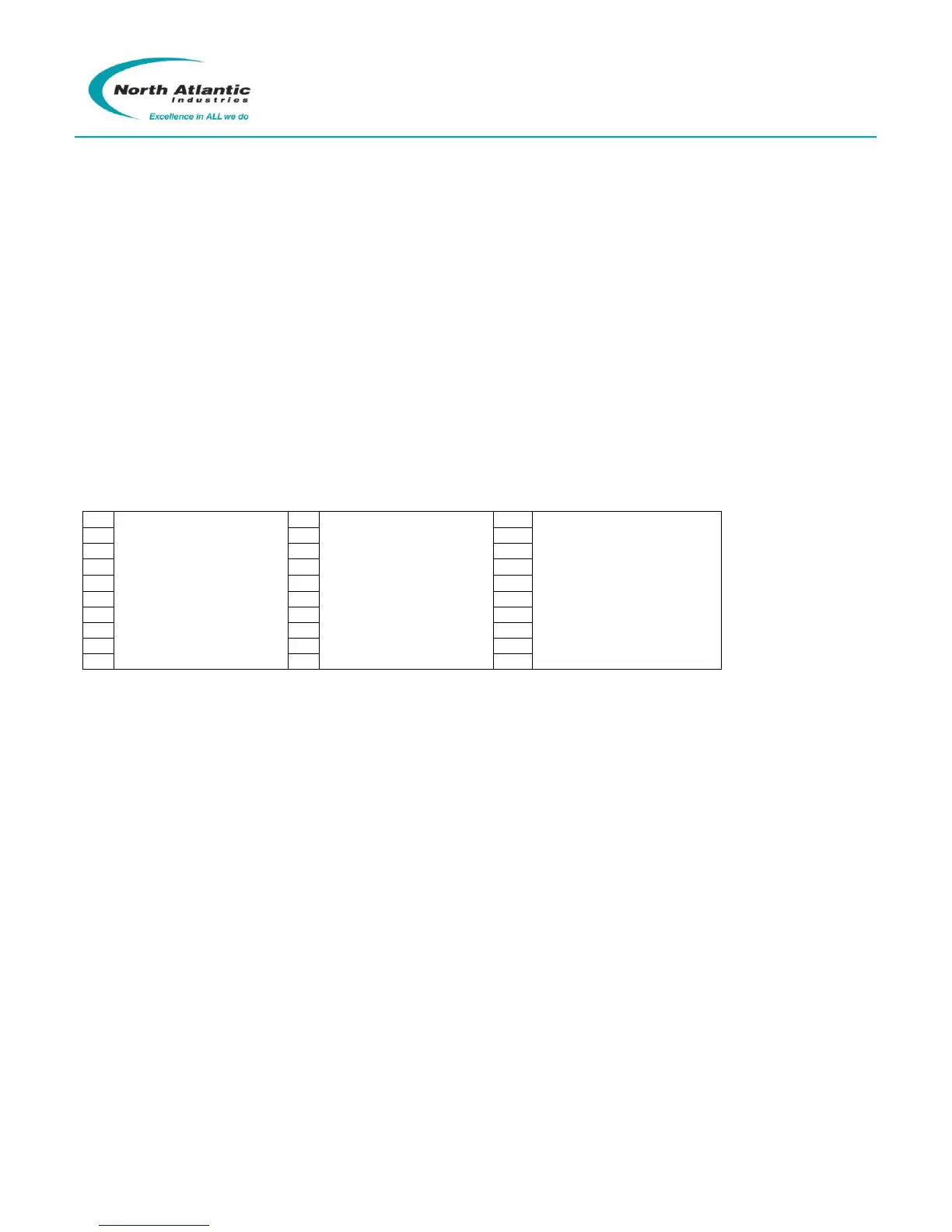
MEMORY MAP
Unit Level General Register…
Any address NOT SPECIFIED within 4096 byte block (up to 3FFFh) is reserved.
The memory map of each module type is described hereafter: