North Atlantic Industries, Inc.
Table of Contents
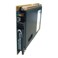
MODEL 75DS2 ...........................................................................................................................................................2
3U CPCI SYNCHRO/RESOLVER OR LVDT/RVDT CONVERTER ..........................................................................2
FEATURES ................................................................................................................................................................2
DESCRIPTION ...........................................................................................................................................................2
SPECIFICATIONS ......................................................................................................................................................6
General – for the Mother Board ............................................................................................................................................... 6
D/S (Module 3*, 4*) – One Isolated Digital-to-SYN/RSL Ch, 3.0 VA Output ............................................................................ 6
D/S (Module 1*,2*) – Two Isolated Digital-to-SYN/RSL Ch, 1.5/2.2 VA Outputs ..................................................................... 6
DLV (Module 5*) – Two/Four Isolated DLV Simulation Ch, LVDT/RVDT Outputs ................................................................... 7
Reference (Module W6, W7)– Optional, Isolated, On-Board Reference Supply ..................................................................... 8
Product Configuration and Memory Map ................................................................................................................................. 9
MEMORY MAP........................................................................................................................................................................ 9
D/S ONE/TWO CHANNEL (MODULES 1*, 2*, 3*, 4*) ............................................................................................ 10
Principle of Operation ............................................................................................................................................................ 10
Built-In Test (BIT) / Diagnostic Capability .............................................................................................................................. 10
Wrap S/D Angle (Read) ......................................................................................................................................................... 11
Measured Reference Voltage ................................................................................................................................................ 11
Measured Signal Voltage ...................................................................................................................................................... 11
Signal Loss Threshold ........................................................................................................................................................... 11
Reference Loss Threshold .................................................................................................................................................... 11
D/S Channel Frequency ........................................................................................................................................................ 11
D/S Status, Signal Loss ......................................................................................................................................................... 12
D/S Wrap Select, Internal/External (Pending) ....................................................................................................................... 12
D/S Status, External Amplifier (Pending) ............................................................................................................................... 12
D/S Write Angle – Single Speed ............................................................................................................................................ 12
D/S Write Angle – Two Speed ............................................................................................................................................... 12
D/S Rotation .......................................................................................................................................................................... 13
D/S Stop Angle ...................................................................................................................................................................... 13
D/S Set Rotation Rate ........................................................................................................................................................... 13
D/S Rotation Mode, Continuous or Start/Stop ....................................................................................................................... 13
D/S Rotation Status ............................................................................................................................................................... 13
Start Rotation ........................................................................................................................................................................ 13
Stop Rotation ......................................................................................................................................................................... 13
D/S Set Reference Voltage ................................................................................................................................................... 14
D/S Set Signal Voltage .......................................................................................................................................................... 14
D/S BIT Test Enable .............................................................................................................................................................. 14
D/S Status, BIT Test .............................................................................................................................................................. 15
Test (D2) Verify ..................................................................................................................................................................... 15
D/S Ratio 1/2 ......................................................................................................................................................................... 15
D/S Output Mode ................................................................................................................................................................... 15
D/S Synchro / Resolver Select .............................................................................................................................................. 16
D/S Torque Receiver Select .................................................................................................................................................. 16
D/S Trigger Source Select ..................................................................................................................................................... 16
D/S Trigger Slope Select ....................................................................................................................................................... 16
D/S Module Power Enable .................................................................................................................................................... 16
D/S Output Enable ................................................................................................................................................................. 16
D/S Active Channel Select .................................................................................................................................................... 17
D/S Status, Reference Loss .................................................................................................................................................. 17
D/S Status, Phase Lock Loss ................................................................................................................................................ 17
D/S Set Phase Offset ............................................................................................................................................................ 17
Reference Loss Interrupt Enable ........................................................................................................................................... 17
Signal Loss Interrupt Enable ................................................................................................................................................. 18
BIT Test Fail Interrupt Enable ................................................................................................................................................ 18
Phase Lock Loss Interrupt Enable ......................................................................................................................................... 18
OSC (Optional Onboard Reference Supply) Set Frequency ................................................................................................. 18
OSC (Optional Onboard Reference Supply) Set Voltage ...................................................................................................... 19
Interrupt Vector ...................................................................................................................................................................... 19
D/S (1*, 2*, 3*, 4*) (PCI) MODULE MEMORY MAP ............................................................................................... 20
DLV TWO/FOUR CHANNEL (MODULE 5*) ........................................................................................................... 21
Principle of Operation ............................................................................................................................................................ 21