FM Transmitter
Sistemas Electrónicos S.A EM 250 COMPACT DIG
Technical Manual - v1.1 - February 2006 19
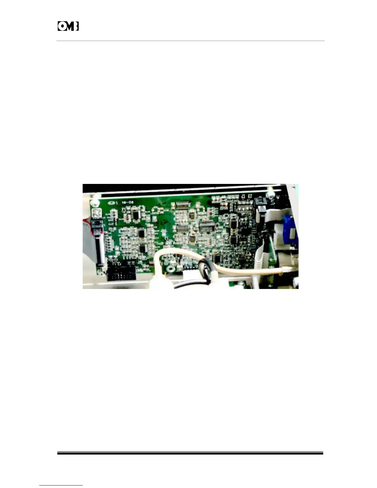
2.2 Audio processor and R.F. control main board.
This is the most complex board in the transmitter and supports the Audio input processing, its level
adjustment, audio-pass filtering and limiting, the RF control section and the I/O interfaces. It also
interconnects the various transmitter modules with ribbon-type cables. Its electrical diagram is splitted
in two sheets for clarity purpose: they will be examined in sequence. In the first Schematics sheet are
situated the I/O interfaces both audio and digital ports and the analog RF control. Let's start to briefly
consider each block diagram.
In the upper left side of the diagram are located the audio channels amplifier/buffers made with 6 op-
amp sections of IC1 and IC2. Two impedance selector jumpers for the audio channels leads the pack
and a protection network made by resistors and diodes protects the inputs from occasional static
discharges,as required for CE compliance.
Four unity-gain active buffers follow and than two balanced to unbalanced signal converters,which
drive the electronic attenuator in the 2
nd
sheet. The last op-amp in IC2 (d),amplify the auxiliary channel
input with a -0.1dB upper corner band >>200kHz and drives the third channel of the electronic
attenuator.
Fig. 2-1: MAIN BOARD IS SITUATED IN THE REAR LEFT SECTION OF CABINET.
On the lower left of the diagram are the RS232 interface (IC5)and the parallel remote I/O active
interface with its protection network, built around TR1, TR2 and TR3. A wired OR pull-up makes the logic
levels <1V as 0 and 10-15V for 1.
On the lower right section of the diagram it is located the RF power controller. The RF forward and
reflected power signals coming from the output directional coupler (this located at RF Power Module)
are amplified by IC3 in a symmetrical circuit. The forward-power control circuit,built around IC4a
continuously drives the RF output stage gain,varying the bias supply voltage to the RF output MOSFET
transistor package. The reflected-power limiting circuit IC4b only acts on the same loop when the IC3b
output voltage is greater than the threshold set by the voltage on the R49/R50 network. A third and
fourth section of IC4 filters and buffers the signal coming from the Microcontroller and set the
reference level for the output power loop. TR4 disables the RF output when the synthesizer is not locked
on the correct frequency.
In the upper right section of the sheet it is shown the control bus connector to the Microcontroller Unit,
which carries the digital control lines on the lower pins and the analog lines on the upper ones. From
this connector comes the power supply too: only +12.5V and -12.5V are used in the board.