AP1302CSSL00SMGAH−GEVB
www.onsemi.com
3
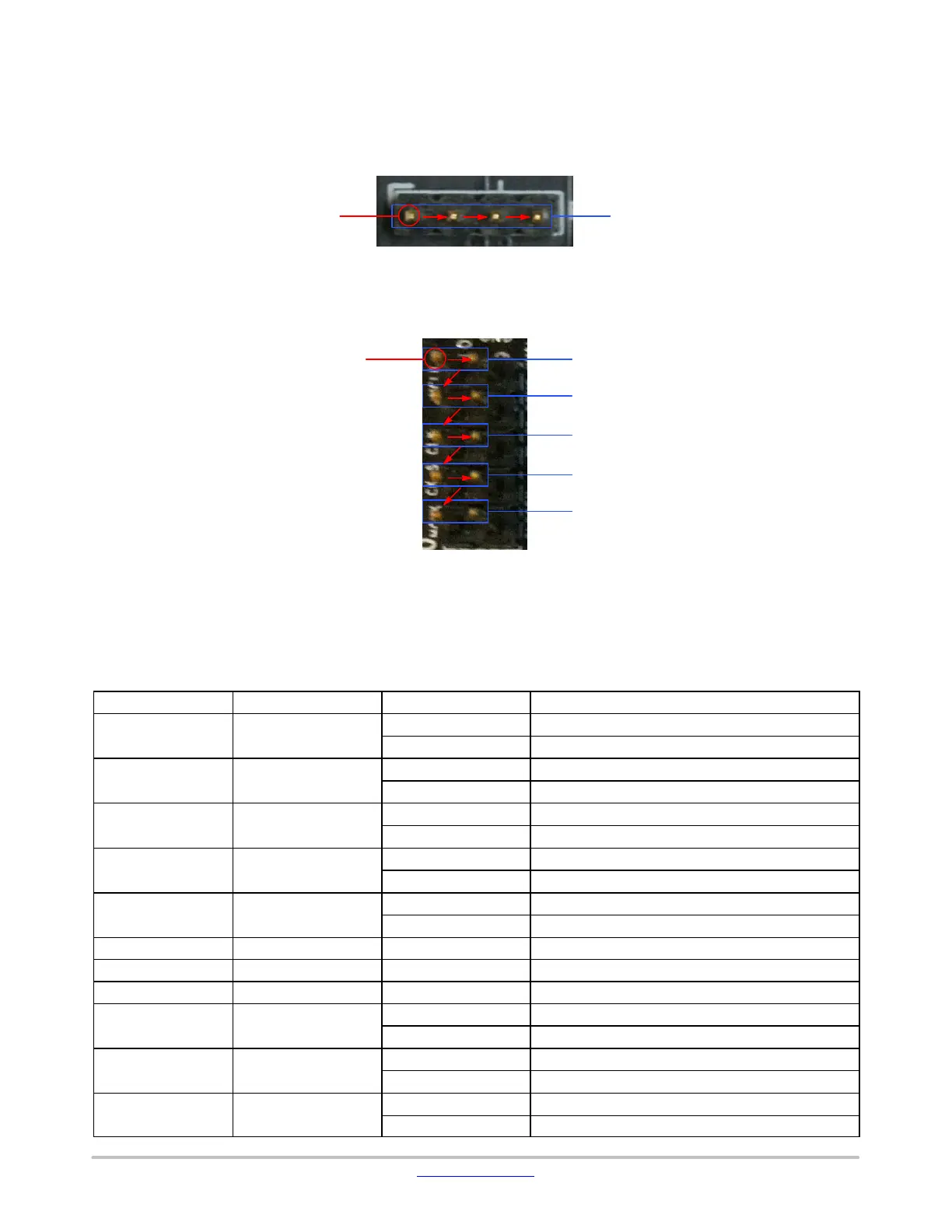
Jumper Pin Locations
The jumpers on headboards start with Pin 1 on the
leftmost side of the pin. Grouped jumpers increase in pin
size with each jumper added.
Figure 5. Pin Locations for a Single Jumper. Pin 1 is Located at the Leftmost Side
and Increases as it Moves to the Right
Pins 1−4Pin 1
Figure 6. Pin Locations and Assignments of Grouped Jumpers.
Pin 1 is Located at the Top-Left Corner and Increases in a Zigzag Fashion Shown in the Picture
Pins 1 and 2Pin 1
Pins 3 and 4
Pins 5 and 6
Pins 7 and 8
Pins 9 and 10
Jumper/Header Functions & Default Positions
Table 1. JUMPERS AND HEADERS
Jumper/Header No.
Jumper/Header Name Pins Description
P1 +5V0 Select
1−2 (Default) Use +5V Supply Source from External Power Adapter
2−3 Use +5V Supply Source from Demo 3 Baseboard
P3 CLK_SELECT
2−3 (Default) Select On-board 48 MHz Oscillator Clock
1−2 Select Clock from Demo 3 Baseboard
P4 I
2
C Debug
1−2 & 3−4 (Default) Connect to Demo 3 Baseboard I
2
C Interface
Open For Connection to External I
2
C Debugger Interface
P5 PRI_I2C_SCL
1−2 (Default) Connect to ICP3 Master SCL
2−3 Connect to Host SCL
P6 PRI_I2C_SCL
1−2 (Default) Connect to ICP3 Master SDA
2−3 Connect to Host SDA
P7 +1V2S Closed (Default) Normal Operation
P8 +1V8S Closed (Default) Normal Operation
P9 +HEADB_1V8S Closed (Default) Normal Operation
P10 I2C_ID Select
1−2 (Default) ICP3 I
2
C Address Set to 0x78
2−3 ICP3 I
2
C Address Set to 0x7A
P12 SEC_I2C_SCL
1−2 (Default) Connect to ICP3 GPIO6 (2ND_I2C_SCL)
2−3 Connect to PRI_I2C_SCL
P13 SEC_I2C_SDA
1−2 (Default) Connect to ICP3 GPIO6 (2ND_I2C_SDA)
2−3 Connect to PRI_I2C_SDA
 Loading...