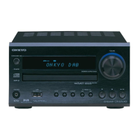
S機種 メインマイコン(M3062LFHPFP)
IC TERMINAL DESCRIPTION CR-325 / 325UKD / 525 / 525UKD
Q701 : MAIN MICROPROCESSOR
No. PIN NAME SIGNAL NAME I/O Act. DESCRIPTION
1 P96/ANEX1/SOUT4 CDDATA O H Command serial data output port to CD signal microprocessor.
2 P95/ANEX0/CLK4 ~CDCLOK O CLK Command transport serial clock output port to CD signal microprocessor.
3 P94/DA1/TB4IN ~CDLAT1 O L Command ratch port to CD signal microprocessor.
4 P93/DA0/TB3IN ~CDRESET O L Reset port for CD signal and MP3 decoder.
5 P92/TB2IN/SOUT3 SUBSDI O H Serial data output port from sub microprocessor.
6 P91/TB1IN/SIN3 SUBSDO I H Serial data input port from sub microprocessor.
7 P90/TB0IN/CLK3 SUBCLK O CLK Serial clock output port to sub microprocessor.
8 BYTE BYTE Ground.
9 CNVSS CNVss Ground.
10 P87/XCIN XCIN Sub clock oscillator port.(32.768kHz)
11 P86/XCOUT XCOUT Sub clock oscillator port.(32.768kHz)
12 ~RESET ~RESET I Reset input port.
13 XOUT Xout Ceramic oscillator port.(6.00MHz)
14 VSS Vss Gound.
15 XIN Xin H Ceramic oscillator port.(6.00MHz)
16 VCC1 Vcc1 Power supply port.
17 P85/~NMI ~NMI I No use.
18 P84/~INT2 ~CDIREQ I L Interrupt request port from CODEC block of the signal processing IC for CD.
19 P83/~INT1 CDACK I H Acknowledging signal input terminal from CODEC block of the signal processing IC for CD.
20 P82/~INT0 ~POFF I L
Power failure/return detection terminal < At the time of WAIT with DOWN, when having a power
failure with UP interruption processing >
21 P81/TA4IN/~U O No use.( Open)
22 P80/TA4OUT/U CDPOWER O H Circuit power source control terminal around CD
23 P77/TA3IN CDFOK I H FOK signal input terminal from of the signal processing IC for CD
24 P76/TA3OUT ~CDLAT2 O L Command latch to CODEC block of the signal processing IC for CD
25 P75/TA2IN/~W ~CDREQ/XTSL O H
Command transfer required signal output terminal to CODEC block of the signal processing IC
for CD. At the time of CXD3059 mode XTSL signal output terminal
26 P74/TA2OUT/W ~SUBRST O H Reset signal output terminal to sub micro-computer
27 P73/~CTS2/~RTS2/TA1IN/~V ~DABRST O L Reset terminal of DAB module
28 P72/CLK2/TA1OUT/V DABPOWER O H DAB module circuit power source control terminal.
29 P71/RXD2/SCL2/TA0IN/TB5IN DABRX I H DAB module serial data entry terminal.
30 P70/TXD2/SDA2/TA0OUT DABTX O H DAB module serial data output terminal.
31 P67/TXD1/SDA1 FTXD O H Port for Flash transfer
32 P66/RXD1/SCL1 FRXD I H Port for Flash transfer
33 P65/CLK1 FCLK O CLK Port for Flash transfer
34
~
~
~
FBUSY O H Port for Flash transfer
35 P63/TXD0/SDA0 CDDATA2O O H
omman
rans
er ser
a
a
a ou
pu
erm
na
o
oc
o
e s
gna
process
ng
or
36 P62/RXD0/SCL0 CDDATA2I I H Serial data entry terminal from CODEC block of the signal processing IC for CD
37 P61/CLK0 ~CDCLOK2 O CLK
omman
rans
er ser
a
c
oc
ou
pu
erm
na
o
oc
o
e s
gna
process
ng
or
w
w
w
.
x
i
a
o
y
u
1
6
3
.
c
o
m
Q
Q
3
7
6
3
1
5
1
5
0
9
9
2
8
9
4
2
9
8
T
E
L
1
3
9
4
2
2
9
6
5
1
3
9
9
2
8
9
4
2
9
8
0
5
1
5
1
3
6
7
3
Q
Q
TEL 13942296513 QQ 376315150 892498299
TEL 13942296513 QQ 376315150 892498299
http://www.xiaoyu163.com
http://www.xiaoyu163.com

 Loading...