EasyManua.ls Logo

Onkyo DX-6830 - Page 16

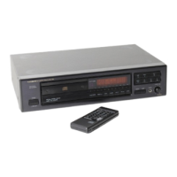
Onkyo DX-6830
24 pages
Print Icon
To Next Page IconTo Next Page
To Previous Page IconTo Previous Page
Loading...
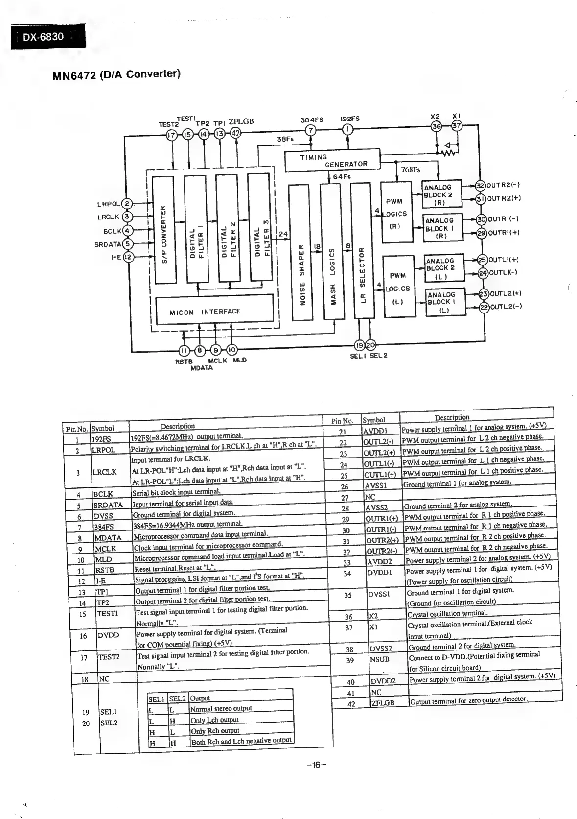
DX-6830
MN6472
(D/A
Converter)
TEST
TEesT2
\
‘tp2
Te)
ZFLGB
384FS
=—«I92FS
x2.
Xi
OUTR2{(-)
LRPOL
Fe
=
ouTR2(t)
LRCLK
WW
SD)
[4
»
BCLK
Sy
a7]
dant
ta
©
TZ
|
les]
(eel
jee
SRDATA
9
rw
re
-
o
o-2
od
os
rE
>
ou
au
ou
NOISE
SHAPER
INTERFACE
RSTB
MCLK
MLD
SEL!
SEL2
MDATA
|
1
__|192Fs
|
2
_\|LRPOL
3
\LRCLK
Polarity
switching
terminal
for
LRCLK.L
ch
at
Input
terminal
for
LRCLK.
At
LR-POL"H":Lch
data
input
at
"H",Reh
data
input
at
"L".
At
LR-POL"L":Lch
data
input
at
"L"
oH".
“HR
chat
"L”
Rech
data
input
at
C]
Q
(wos
nw
f
ae
DVSS
Ground
terminal
for
digital
system.
)
28
|
Ground
terminal
2
for
analog
system.
pvss__|
2
|
9
|
K
Clock
input
terminal
for
microprocessor
command.
3
|
‘Microprocessor
command
load
input
terminal.Load
at"L".
|
command
load
input
terminal.Load
at
“Ls
32
|
processing
LSI
format
at
Reset
terminal.Reset
at
"L
g
"L"
and
IS
format
at
"H",
mere
—
ee
Output
terminal
1
for
digital
filter
portion
test.
Power
supply
for
oscillation
circuit
14
Test
signal
input
terminal
1
for
testing
digital
filter
portion.
Ground
for
oscillation
circuit
seer
osciation
ermine,
i
ing
input
terminal
=
re
ee
)
nn
sy
w
41
ZFLGB
Output
terminal
for
zero
output
detector.
-16-
192FS(=8.4672MHz)
output
terminal.
ear
TTAVDDI.
[Power
supoly
tering
1
fr
analog
system.
(459)
|
Four
2c)
[PWM
output
ermina
for
L2
ch
negative
pase._|
(OUTL
200)
[PWM
output
terminal
for
L2.ch
psiive
pase.
_|
Fe
Tour
PWM
ouput
ermina
for
LI
ch
negative
pase.
(OUTL1Ca)
[PWM
output
terminal
for
L
1
ch
psiive
phase.
_|
Serial
bit
clock
input
terminal.
ATA
Se
a
ae
3
_|avss2
_|
OUTRIGD
[PWM
output
terminal
for
RI
ch
postive
phase.
_|
fers
pss
ma
i
Four
evo
emia
Btn
lowrRa(e)
[PWM
ouput
ermina
for
R
2
ch
positive
phase.
_|
OUTR2()
[PWM
output
erminal
for
R
2
ch
negative
phase_|
|
38
_|pvss2__|
Ground
terminal
2
for
digital
system.
39
NSUB
Connect
to
D-VDD.(Potential
fixing
terminal
;
for
Silicon
circuit
board)
T
40
|
DVDD2
Power
supply
terminal
2
for_di
gital
system.
(+5V)_}