EasyManua.ls Logo

Onkyo DX-7511

Onkyo DX-7511
23 pages
To Next Page IconTo Next Page
Loading...
Ref.
No.3567
SERVICE
MANUAL
|
COMPACT
DISC
PLAYER
DX-7511
Black
model/Silver
model
MP,MPT
_
230V
AC,50Hz
_
120/220V
AC,
50/60Hz
|
SAFETY-RELATED
COMPONENT
WARNING!
Specifications
COMPONENTS
IDENTIFIED
BY
MARK
A\
ON
THE
——
Signal
readout
system:
Optical
non-conta
SCHEMATIC
DIAGRAM
ANDINTHEPARTSLISTARE
—Reaingrotation:
About
$00-
200
rpm.
CRITICAL
FOR
RISK
OF
FIRE
AND
ELECTRIC
SHOCK.
|
)
eo
|
Linear
velocity:
1.2-
1.4
m/s
:
REPLACE
THESE
COMPONENTS
WITH
ONKYO
Error
correction
system:
Cross
Interleave
Reed-Solomon
cod
|
|
D/A
converter:
1
bit
PWM
ACCUPULSE
D/A
PARTS
WHOSE
PART
NUMBERS
APPEAR
AS
SHOWN
|
CONVERTER
©
|
|
|
Sampling
frequency:
352.8
kHz
(Eight-times
IN
THIS
MANUAL.
;
oversampling)
-
_
Number
of
channels:
2
(stereo)
_
|
Frequency
response:
5
Hz
-
20
kHz
MAKE
LEA
KAGE-CURRENT
OR
RESISTANCE
Total
harmonic
distortion:
0.004
%
(at
1
kHz)
Dynamic
range:
96dB
MEASUREMENTS
TO
DETERMINE
THAT
EXPOSED
Sal
wosteamie:
*
ro
PARTS
ARE
ACCEPTABLY
INSULATED
FROM
THE
Channel
separation:
90
dB
(at
I
kHz)
|
|
Wow
and
Flutter:
Below
threshold
of
measurability
SUPPLY
CIRCUIT
BEFORE
RETURNING
THE
Output
level:
2
volts
r.m.s.
:
|
:
7
Headphone
jack:
1
APPLIANCE
TO
THE
CUSTOMER.
Opdinum
Ina
impedance
8
to
200
ohms
Power
consumption:
15
watts
Power
supply
rating:
European
and
Australian
models:
)
|
AC
230
V,
50
Hz
,
Worldwide
model:
|
AC
120
V
and
AC
220-230V
KYO
switchable,
50/60
Hz
,
®
Dimensions
(Wx
H
xD):
435
x
121.
x
310
mm
(17-1/8"
x
4-3/4"
x
12-3/16")
Weight:
4,7
kg
(10.4
Ibs.)
Specifications
and
external
appearance
are
subject
to
change
without
notice
because
of
product
improvements.
AUDIO
COMPONENTS
Question and Answer IconNeed help?

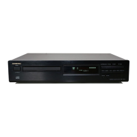
Do you have a question about the Onkyo DX-7511 and is the answer not in the manual?

Onkyo DX-7511 Specifications

General IconGeneral
BrandOnkyo
ModelDX-7511
CategoryCD Player
LanguageEnglish

Summary

SAFETY-RELATED COMPONENT WARNING!

Specifications

SERVICE PROCEDURES AND PRECAUTIONS

Safety Checks and Voltage Settings

Covers safety-out procedures, voltage selector usage, and optical pickup handling cautions.

General Servicing Precautions

Includes grounding guidelines, handling sensitive components, and other general safety measures.

LASER SAFETY DURING SERVICING

Eye Protection Guidelines

Instructions to avoid direct laser beam exposure and observe from a safe distance.

Laser Warning Label Identification

Displays various warning labels related to laser radiation found on the unit.

CHASSIS - EXPLODED VIEW

CHASSIS - EXPLODED VIEW PARTS LIST

CD MECHANISM EXPLODED VIEW

CD MECHANISM PARTS LIST

DRIVE UNIT EXPLODED VIEW

DRIVE UNIT PARTS LIST

IC BLOCK DIAGRAMS AND DESCRIPTION

IC PIN DESCRIPTIONS AND DIAGRAMS

CXA1571 S (RF Amp) Circuit Diagram

CXA1372 Q (Servo Signal Processor) Diagram

BA6398 FP and LH5164 AN-10 L Diagrams

SM5872 CN (DA converter) Diagram

TA7291 Diagram and Operation Table

SYSTEM BLOCK DIAGRAM AND MICROPROCESSOR DETAILS

System Block Diagram

Overall system block diagram showing interconnected modules and ICs.

Microprocessor Terminal Description

Detailed pin descriptions for the µPD78042FGF-034 microprocessor.

ADJUSTMENT PROCEDURES - Part 1

Focus Offset Adjustment

Procedure to adjust R119 for maximum waveform on terminal P105.

Tracking Offset Adjustment

Procedure to adjust R116 for GND level tracking error signal.

ADJUSTMENT PROCEDURES - Part 2

Focus Gain Adjustment

Procedure to adjust R120 for equal 800Hz components on oscilloscope channels.

Tracking Gain Adjustment

Procedure to adjust R121 for equal 1.2kHz components on oscilloscope channels.

PRINTED CIRCUIT BOARD VIEW FROM BOTTOM SIDE

PRINTED CIRCUIT BOARD PARTS LIST (MAIN CIRCUIT)

PRINTED CIRCUIT BOARD PARTS LIST (OTHER BOARDS)

PACKING VIEW

PARTS LIST (PACKING)

Related product manuals