Pin
No.
Port Description I/O (V)
FM AM CD
94 NC - - - - -
95 OSC
FM/AM
FM/AM osc input I 1.4 1.3 1.3
96
VSSPLL
Ground - 0 0 0
97 NC - - - - -
98 EO1 PLL phase
comparison error
output
O 2.2 2.1 2.3
99 TEST1 Ground I 0 0 0
100 XOUT Crystal oscillator O 2.6 2.6 2.6
9.2. Display Block
IC901 : C0HBA0000195
Pin
No.
Port Description I/O (V)
1 GREEN
CNT
LED control (Green) O 0
2 RED CNT LED control (Red) O 4.9
3 -39 SEG3 -39 LCD segment data O 2.5
40 -43 COM1 -4 LCD common O 2.5
44, 45 SEG40,
41
LCD segment data O 2.5
46 -49 KS3-6 Key scan O 5.0
50 -54 Kl1-5 Key data I 0
55 TEST (Connecting to ground) - 0
56 VDD +5V power supply - 5.0
57 VDD1 VDD1 filter terminal - 3.3
58 VDD2 VDD2 filter terminal - 1.7
59 VSS Ground - 0
60 OSC Oscillator terminal - 3.8
61 DO Key data output O 5.0
62 CE LCD driver chip enable I 0.3
63 CLK LCD clock I 5.1
64 DI LCD data I 4.9
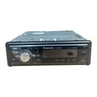
10. PACKAGE AND IC BLOCK DIAGRAM
10.1. Main Block
PA051 : YESAP403
9
 Loading...