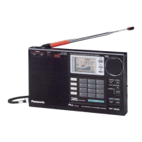
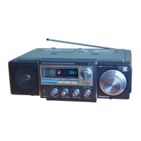
RF·B600u RF·B600!
'.
PLL
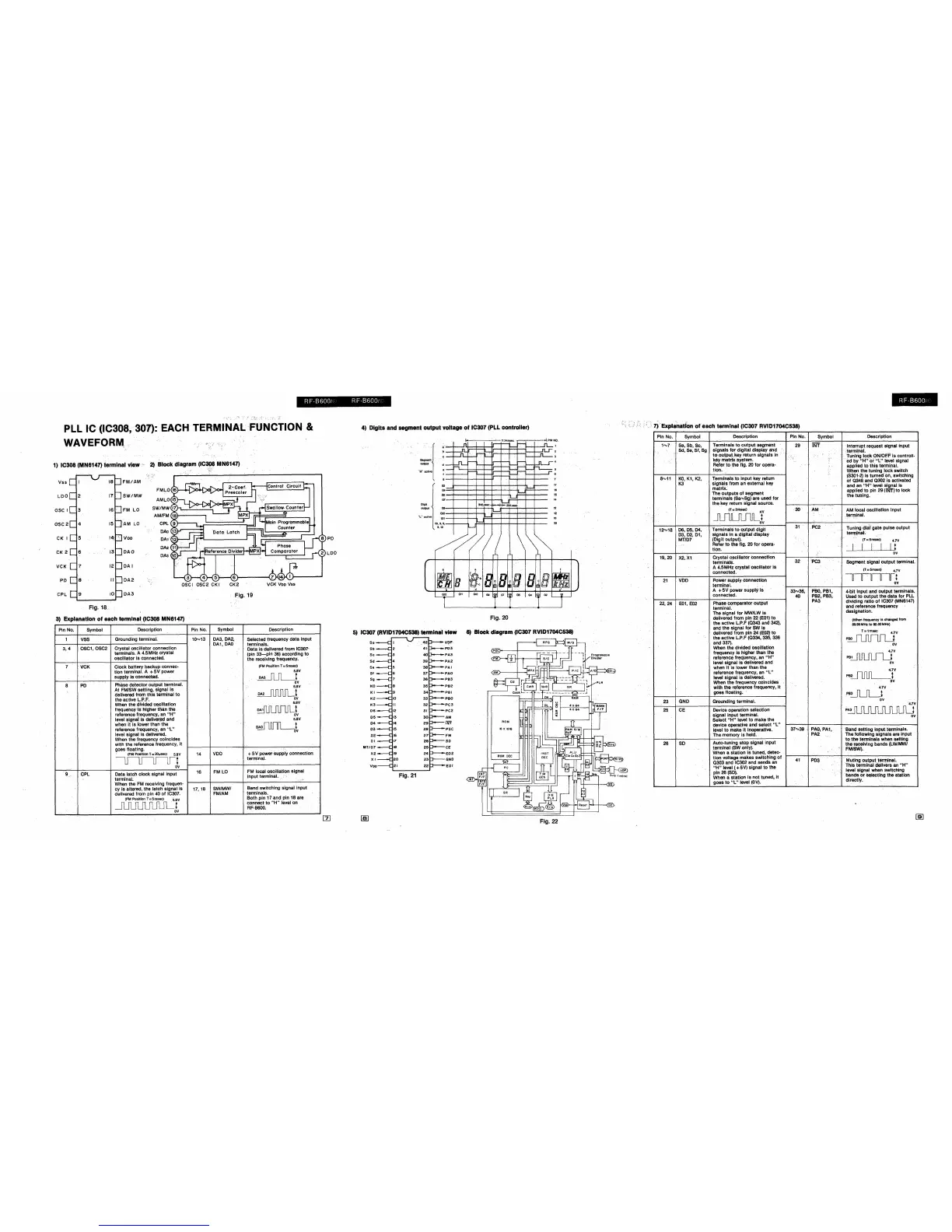
IC (lCS68,S07):EACH TERM'INALFUNCTIONI:
WAVEFORM:.
1)
lC30e
(MN$141) ferminal
vie.'
2).
Stock diagram
(1C~
MN6141)
MfOl Citcuit
SW/MW
FM
LO
AM
LO
Voo
DAO
GA.
1
DA2
Fig. 18.
3)
Explanation
of
each termlnal'(IC308 MN6141)
Pin
Ho.
Symbol
3,"
0001,0002
.
7 \let<
'El
PD
'.
9.
CPt
.
..
Description
Groundi·ng terminal.
Crystal
oscillator oonnecfion
termtnals. A
4.5
MHz crystal
o$cillator
'1$
cOllneoted.
Clock battery backl.l(l cànnec-
tion
terminal. A +
SV
power
suppl}' Iseon nlfro\$d.
'.
Phàse detectoroutput
termin.at.
At
FMJSWsetting, s.igllalls
deliVered from thi& terminal
10
the
activeL..P.f.
Whefl
the
dfVidèdOl.!!::lftatlon
frequedcYfl!Il'fignet thân the
refereneefrequenGY;all "HU
level $,iunali.s
Ueliver~and
when
ii
Is
IOwer
than the
referenœ
frequ~mcy,
an"!.."
Ie.vel
.
ails
dertllered.
Whan ney cOïncides
wnh
1he ce frequency,
lt
1O'V13
DA3,I>A2,
DA1,DAO
Oe.scriptÎon
Sfllectedlrequen.cy
data.
_"put
terminais,
Data
1$~lvered
from
10861
(pin
33-pin
36)
according
\0
the receMng frequency •
(FM
Po$illon T "lim$ltq).
5.8'1
~t
IlV
uv
~J
eV
S.av
~t
QV
5.lIV
~t
OV
.
goe.$
rloating.
voo
...•.
.
+.sV powet'$upply ccnnection.
terminal.
.
(FM
PositiOll T =
20_0)
5.IlV
14
UL~t
QV
FM
(ooal
oscillation signal
Input terminal. .
FMLO
16
Data tatotl cl,ookslgnal Input
terminai.>
When the
FM
receiving frequen-
}----+-----I---------~---~--.,-:..-;
cy
i.s
altemd, the latoh signal Is
17,
18SW/MWI
Band .swltching signal input
dellve.red fram pin
40
of
1C307.
FM/AM
tel1T1inals.
(f'MPo$idonr"5m,,e~j
.
i;.8I1Bolh.pin
17and
ptn 18
are
.
n ri n n n nUL.. t connect
to"H"
leve] on
--.J U U U U U i
RF'BmlO.·
'.
ov
4) Digits and segment outpUt voltage
of
10307
(PlL
contraller)
5)IC301 (RYI01704C638)terminalvlew
SQ'---i:l
Sb
S"
Sel
s.
Sf
Sg
I<t)
1<1
1<2
1<3
06
015
.114
03
D2---1L1
DI
M1I01
---iC1
)(2
XI
Fig.
21
lI.M
iVf
PSC
FM
SD
CE
E02
SNI)
Eol
.
Fig.
20
6)
Block dlagram(lC307
RVlD1T04C538)
FIg.
22
'.
RF·B6001 (
7)Expla\1àtÎ0n
of
.ach
terminai
(1C307
RVIDtT04OS38)
Ptn No. Symbol
,,,-,7
Sa,
Sb,
sc,
<
$d,
SQ.Sf,SQ
S'V
1'1
KO,
K1,
K2,
K3
12'viS 06, 05, 04,
OS,D2.,
Dl,
MT/OY
[.
21
VDO
22,
2.4
6)1,e02
23
GND
25
CE
.
26
SO
Description
Termlnals
to
output
segment
slgnalstord!gjtal
dl$pfay âIld
..
'.
tQcoutPU~,
keyraturn signais .in '
••
kèy
matrixs,ystem. '
Reter.1O
t\'I$
fig.
20
fOr
opera-
tiOn;
."
.
Termlllals.to input
key
fatum
signaIs from an 'IIxtemal
key
maftl}(. .
The outputs
of
segment
terminais lSa'VSgl
are.
u&ed
for
the key fatum signai source.
.
.lh'2",_)
!IV
~+
av
Term.inalà
tOQutpul
di.git
Signais
in
aqlgltat
dispfay
(DIgit outpl.lt).
.•
Aefer
ta thef!g,
20
for
opera·
tion.
Crystal oscutatôr
oonne.oUon
terminais •
A
4.5MHZ
ctystaioseUlator
1$
con ne:eted. .
'.
29
!NT
..
'.
.
.
lnterrupt requast
slQnai
Input
."
ter~~1.
TunÎng lookONIOI7F
Is
contrOlI.
.
éd
Ily
"H"
or
"L"
~el$lgnal
appUed
lo
thistermi.nal.
When the tuning lock swilch
(S3Q1
c
2)
ls
turned
on,
swftchlng
ofQ34Band Q302ls
acUvated
andan"H"
leva!
algnalls
appHedto
pin
29 (TNTlto lock
t.h'll
tunlng.
AM
local oscillallonlnput
tertl'lirtal.
.
Tunlng (Jfafgata pulseoolpl.lt
l'efrnlnat;
(T"
SI'/islKlI
1 1 1
.
(T
..
5m!lllc)
4,7V
",urrrT:
Power supply
eOnne.ot1on
terminal.
A
....
SV
power suppl)'
1$
connec1ed"
'~
___
~'~~~.
____
-4~
_______________
~_V
____
-;
33tvs6,
p~,
PB1.
PIlaseOQmparator
outpUt
lermlnal.
The
stgnalfor
MWllW
Is
de[lvered lrom
pm
22
(EQ1)
ta
the
active
LP.F
(Q&13
and 342),
and
the
signai for
SW
is
deUvered
from pin
24
(EQ2)1O
the active LP.F{Q334, 335,
336
and (31).
When
the
dlVl<led
oscillation
frequency
ls
hlgber Ihan. the
refer~mce
freqQency,
an
"H"
levai signal Is dellveredand
whan it is lower Ihan
the
re.fe.rence
freque.ncy,
an
"l"
levai.
signalis
dell.vered.
When the fmquenoyoolncides
wllh
tJle
ret~rencefrequency.
if.
goesfloat!ng.
Gi'o.l,IIldlng·
t.ermînal.
..
Devlcè
operation
sefectlOl1
s.ignal
in.put
terminal.
Séleot
"H"
lévalto
ma.ke
t.he
devlOé
®erattve and select .iL"
teveI
to
maké
il
inoperaWe.
The memory is hetd.
Auto-tunlngstopslgnal
input
terminal
.(SW
on1y).
Wtlén a
IiltaUon
Is
ttlne.d, delec-
tlon voltage makes swltohing
o.f
Q.303
and
10302
and
sends
an
"H"
levaI
(+5Vl
signal
10
the
pin
26
(SOl.
Wh.en
a
s1aHon
Is
not
tun'lld,
it
goes
10
"L."
leVéI
((l'l).
1
.
40
P82,
Pt!i3,
PAS
37"'39
41
PA,O,PA1,
PA2
PO~
.
".
.
..
. " .
'.
4.olt input and outpUt terminais
•.
Used
ta
out
pl.ltthe
dam
fer
PLL
dlvldlng
ratio
of
10307
(M1\I61411
and
refetenœ freqÎlèllCy
desiV
natlOl1
.
lWhen
II$luilll~
is
~an;glId
-
89.9li
MHz
to
1lO.00MHzj
""lm$$l;
4.7V
P~
~V
4.1V
PB.wJLIlSL:
ov
4.1\1
PB2~t
DV
Bal'ldsetting Inputtermlnals.
Thé.foIJoW*ng
signais
are.
input
tott\e~erminal{l
wMn
seHin{J
thé recelvlng bands
(LW/MWI
'.'
FMI$W).
i Mut/ng outpulten"!lina.l.
. Tllls terminaI
delMrs
an"H"
levai
signll! when switching
bands
o'$t!eetlng
thestaUon
direetty.
' .
.
.'
.