Do you have a question about the Panasonic SA-EH60X and is the answer not in the manual?
Detailed specifications for the amplifier section, including power output and distortion.
FM and AM tuner specifications, covering frequency range, sensitivity, and S/N.
Power consumption, supply voltage, dimensions, and weight of the unit.
Critical warning for technicians regarding electrical hazards and safe servicing practices.
Instructions for safely discharging power supply capacitors and checking primary voltage.
Explains the function of the protection circuitry and provides troubleshooting steps for activation.
Lists all included accessories such as power cords, antennas, and remote control.
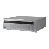
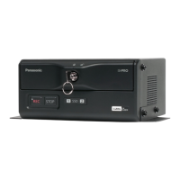
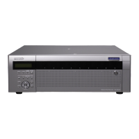
Identifies and describes the function of each button and jack on the front panel.
Instructions for battery installation and proper usage of the remote control.
Guidelines for stacking system components and optimal speaker placement.
Steps for connecting front, surround, and center speakers, plus final AC power connection.
Procedure for connecting the unit for Video CD playback to a TV.
Instructions for connecting flat cables, FM indoor, and AM loop antennas.
Details on speaker wiring, center speaker connection, and Video CD output settings.
Guidelines for connecting external components and antennas, including safety notes.
Wiring diagrams for connecting the sound processor and TV via AV cables.
Connection methods for VCR, CD player, cassette deck, and turntable.
Step-by-step instructions for setting the 24-hour clock display accurately.
Information on how the demo function operates and how to disable it.
Introduction to inspection and replacement procedures, with notes on reassembly.
Index listing inspection procedures for various circuit boards within the unit.
Index for procedures related to replacing power ICs and regulator transistors.
Instructions for inspecting the tuner, Dolby, and power supply circuit boards.
Steps required to inspect the operation circuit board.
Steps required to inspect the main circuit board assembly.
Steps for removing the heat sink unit and disconnecting various connectors.
Procedure for sliding out and removing the main printed circuit board.
Steps for reinstalling the input/output board and connecting wires.
Detailed instructions for replacing power ICs and regulator transistors, including thermal grease application.
Steps for removing connectors and replacing transistor holders.
Procedure for supplying power to the unit and performing basic operational checks.
Steps to verify the karaoke function using the sound processor.
Explains how error codes are displayed and interpreted for fault diagnosis.
Provides methods for resolving specific error codes like U-70 and F-61.
Lists schematics for tuner, operation, and microphone jack circuits.
Lists schematics for Dolby, terminal, main, and power supply circuits.
Lists schematics for power transformer and V. Mute circuits.
Explains notes, symbols, voltage/signal line indicators, and safety notices.
Schematic diagram of the FM/AM front end circuitry, including RF amplifier.
Schematic diagram of the PLL frequency synthesizer and associated oscillator circuits.
Schematic diagram detailing the FM IF amplifier and decoder stages.
Diagram illustrating FM/AM signal paths and control signal lines.
Schematic of the FL display driver and the system control IC (IC901).
Schematic showing the routing of signals from front panel keys to the system control IC.
Schematic of the microphone amplifier circuit and volume controls.
Schematic showing the remote sensor and tuner band select signal paths.
Schematic diagram of the Dolby Pro Logic IC (IC801) and its internal signal processing blocks.
Schematic illustrating the electric volume control and microcomputer interface circuits.
Schematics detailing the muting control and attenuator circuits for audio signals.
Schematic diagram for the phono input and external input/output terminal circuits.
Diagram showing control signal connections from terminals to the main circuit.
Wiring diagrams showing connections between the main circuit and operation/Dolby circuits.
Wiring diagrams showing connections to the tuner and power transformer circuits.
Schematic diagram for the digital sound controller IC (IC301).
Schematic diagram of the graphic equalizer and microcomputer interface sections.
Schematic diagrams for muting control and audio attenuator circuits.
Schematic diagrams for the filter amplifier IC and motor drive circuits.
Schematic diagrams for the power amplifier IC and various voltage regulator circuits.
Schematic diagrams for the FL (Fluorescent Display) driver circuits.
Schematic diagrams for the primary and secondary power transformers.
Schematic diagram detailing the power supply circuitry, including regulators and relays.
Schematics showing speaker output connections and relay drive circuits.
Schematic diagram of the V. Mute circuit, including muting control transistors and buffer amplifier.
Physical layout diagram of the tuner printed circuit board.
Physical layout diagram of the operation printed circuit board.
Physical layout diagram of the main printed circuit board.
Physical layout diagram of the Dolby Pro Logic printed circuit board.
Physical layout diagrams for power supply, V. Mute, and mic jack circuit boards.
Physical layout diagram of the input/output terminal printed circuit board.
Visual representations of various integrated circuits, transistors, and diodes used in the unit.
Diagram showing the interconnections between major circuit boards and components.
Detailed wiring connections for connectors on various printed circuit boards.
Detailed description of the terminal functions for IC901 (System Control).
Block diagram illustrating the tuner front-end and PLL frequency synthesizer functions.
Block diagram of the digital sound controller and microcomputer interface sections.
Block diagram illustrating the signal flow and processing within the Dolby Pro Logic section.
Block diagram showing the electric volume control and filter amplifier sections.
Block diagram illustrating the power amplifier stages and motor drive control.
Block diagram illustrating the power supply and voltage regulator circuits.
List of replacement integrated circuits with part numbers and remarks.
List of replacement transistors, continuing from previous section.
Continuation of the list of replacement transistors with part numbers.
List of replacement diodes, coils, filters, transformers, and oscillators.
List of replacement display tubes, fuses, variable resistors, and connectors.
List of replacement connectors, earth terminals, fuse holders, relays, and jacks.
List of replacement antennas, system parts, and other miscellaneous components.
List of replacement resistors in the R103 to R258 range with values and remarks.
List of replacement resistors in the R301 to R421 range with values and remarks.
List of replacement resistors in the R602 to R975 range with values and remarks.
List of replacement capacitors C101 to C103 with values and remarks.
List of replacement capacitors in the C103 to C353 range with values and remarks.
List of replacement capacitors in the C354 to C734 range with values and remarks.
List of replacement capacitors in the C734 to C1111 range with values and remarks.
List of cabinet parts, including screws, knobs, and panels.
List of accessories, packing materials, and jigs/tools included with the unit.
Diagram showing the physical location and reference numbers for cabinet parts.
Diagrams illustrating the correct packaging procedure for different system units.
Diagram showing how the included accessories should be packaged.
| Brand | Panasonic |
|---|---|
| Model | SA-EH60X |
| Frequency Response | 20Hz - 20kHz |
| Tuning range | FM |
| FM Tuning range | 87.5 - 108.0 MHz |
| Speaker Impedance | 6Ω |