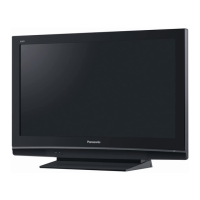
Do you have a question about the Panasonic TH-37PX80B and is the answer not in the manual?
General guidelines for servicing, including lead dress, protective devices, and leakage current checks.
Procedure for checking touch currents, including measuring network and voltage limits.
Techniques to reduce component damage from static electricity during handling and installation.
Information on lead-free solder composition, usage, and precautions for PCB assembly and service.
Details on component board names and their functions for 42-inch models, including chassis removal.
Details on component board names and their functions for 37-inch models, including chassis removal.
Lists applicable video signals for PC input, including horizontal and vertical frequencies.
Instructions on how to access the service mode using the main unit and remote control buttons.
Explanation of button commands used within the service mode for navigation and value adjustment.
Lists the adjustable items within the service mode, showing sub-items, sample data, and remarks.
Instructions on how to exit the service mode by powering off the unit or remote control.
How to access and use the service tool mode for checking SOS history and power on time/count.
Steps to access the service tool mode from the main service mode.
Explanation of the SOS history indication and how it is cleared.
How to display and interpret power on time and count data.
Instructions on how to exit the service tool mode.
Purpose, access command, and explanation of the hotel mode setup menu for restricting functions.
Procedure to check IIC bus lines and screen display status for troubleshooting.
Steps to access the IIC bus line check through the self-check function.
Example screen display for the IIC bus line check.
Points to check if an NG (Not Good) status is displayed in the IIC bus check.
Instructions on how to exit the IIC bus line check.
Chart detailing power LED blinking patterns and their corresponding error causes and related boards.
Troubleshooting guide for no power indication, outlining states and check points for P board or A board.
Troubleshooting flowchart for no picture issues, guiding through checks for OSD, SC board, and SS board.
Explanation of local screen failure on plasma display and possible defective PCBs indicated by Fig-1.
Instructions on how to remove the rear cover, referring to Service Hint section 3.
Steps for removing the P-Board, including safety precautions for capacitor discharge.
Instructions for removing the rear terminal cover, detailing screw removal.
Steps for removing the tuner unit, including cable and connector disconnection.
Instructions for removing the A-Board, involving tuner unit removal and cover detachment.
Procedure for removing the SU-Board for 42-inch models, detailing flexible cable and screw removal.
Procedure for removing the SM-Board for 37-inch models, detailing flexible cable and screw removal.
Procedure for removing the SD-Board for 42-inch models, detailing flexible cable and screw removal.
Steps for removing the SC-Board, including disconnection of other boards and cables.
Procedure for removing the SS-Board, including cable clampers, connectors, flexible cables, and screws.
Instructions for removing the left and right stand brackets from the plasma panel.
Procedure for removing the C1-Board, involving tuner unit removal and flexible cable disconnection.
Procedure for removing the C2-Board, involving tuner unit removal and flexible cable disconnection.
Steps for removing the front shield unit assembly, including connector and screw removal.
Procedure for removing the G-Board and GS-Board, involving front bracket and shield unit removal.
Instructions for removing the left and right speakers, including connector and screw removal.
Procedure for removing the S-Board, including stand bracket removal and connector disconnection.
Steps for removing the K-Board, including S-Board removal and connector disconnection.
Procedure for removing the plasma panel section from the cabinet assembly, including stand bracket and spacer removal.
Instructions for replacing the plasma panel, covering board attachment, cable connection, and fitting.
Preparation steps for driver setup, including input signal and picture control settings.
Items and preparation steps required for driver setup, including caution notes on adjustment order.
List of voltages to check or adjust with a multimeter, referring to panel data label.
Cautions and quick adjustment procedures after exchanging Printed Circuit Boards.
Cautionary notes before removing PCBs, regarding capacitor discharge time.
Guidelines for quick adjustment after PCB exchange, including voltage checks and cautions.
Diagram showing the location of adjustment volumes on the circuit boards.
Diagram indicating the location of test points for voltage measurements on various boards.
Detailed block diagram showing the interconnections of main functional blocks and components.
Block diagram illustrating the system architecture for 42-inch models, detailing power supply and board connections.
Block diagram illustrating the system architecture for 37-inch models, detailing power supply and board connections.
Block diagram detailing signal paths and connections for audio, video, PC, and HDMI interfaces.
Block diagram illustrating the interconnections of the main MCU, memory, and interface circuits.
Block diagram showing the connection between the main board, power supply, and plasma panel drivers.
Block diagram showing the connection between the main board, power supply, and plasma panel drivers for 37-inch models.
Important caution regarding correct assembly and locking of flexible cables in connectors.
Wiring diagrams and cable routing information for 42-inch models.
Wiring diagrams and cable routing information for 37-inch models.
Notes and explanations for understanding schematic diagrams, including component identification and symbols.
Schematic diagram for the P-Board (part 1 of 6), showing connections for Europe and Asia models.
Schematic diagram for the P-Board (part 2 of 6), showing power control and board connections.
Schematic diagram for the P-Board (part 3 of 6), illustrating photo coupler and error detection circuits.
Schematic diagram for the P-Board (part 4 of 6), showing connections to SC-Board and SS-Board.
Schematic diagram for the P-Board (part 5 of 6), showing connections to power MCU and other circuits.
Schematic diagram for the P-Board (part 6 of 6), showing DC-DC converters and connections to A-Board.
Schematic diagrams for G, GS, and K-Boards, illustrating their internal circuitry and connections.
Schematic diagram for the A-Board (part 1/19), showing IIC connections and tuner interface.
Schematic diagram for the A-Board (part 2/19), detailing DDR memory interface and connections.
Schematic diagram for the A-Board (part 3/19), showing various I/O ports and signal processing circuits.
Schematic diagram for the A-Board (part 4/19), illustrating connections for audio, HDMI, and tuner signals.
Schematic diagram for the A-Board (part 5/19), showing DC-DC converter circuits and power management.
Schematic diagram for the A-Board (part 6/19), detailing connections for various control signals and interfaces.
Schematic diagram for the A-Board (part 7/19), showing connections for display drivers and panel interface.
Schematic diagram for the A-Board (part 8/19), detailing connections for PC signals and external interfaces.
Schematic diagram for the A-Board (part 9/19), showing connections for JTAG interface and other control signals.
Schematic diagram for the A-Board (part 10/19), illustrating audio output and input connections.
Schematic diagram for the A-Board (part 11/19), showing connections for various input/output terminals and power management.
Schematic diagram for the A-Board (part 12/19), illustrating DC-DC converters and power supply connections.
Schematic diagram for the A-Board (part 13/19), showing connections for various control signals and interfaces.
Schematic diagram for the A-Board (part 14/19), detailing connections for audio and PC signals.
Schematic diagram for the A-Board (part 15/19), showing connections for display drivers and DDR memory interface.
Schematic diagram for the A-Board (part 16/19), illustrating connections for display drivers and LVDS interface.
Schematic diagram for the A-Board (part 17/19), showing connections for DDR memory interface and display drivers.
Schematic diagram for the A-Board (part 18/19), detailing connections for audio and control signals.
Schematic diagram for the A-Board (part 19/19), illustrating connections for display drivers and control logic.
Schematic diagram for the C1-Board (part 1/2) for 42-inch models, showing driver and data connections.
Schematic diagram for the C1-Board (part 2/2) for 42-inch models, showing driver and data connections.
Schematic diagram for the C1-Board (part 1/2) for 37-inch models, showing driver and data connections.
Schematic diagram for the C1-Board (part 2/2) for 37-inch models, showing driver and data connections.
Schematic diagram for the C2-Board (part 1/2) for 42-inch models, showing driver and data connections.
Schematic diagram for the C2-Board (part 2/2) for 42-inch models, showing driver and data connections.
Schematic diagram for the C2-Board (part 1/2) for 37-inch models, showing driver and data connections.
Schematic diagram for the C2-Board (part 2/2) for 37-inch models, showing driver and data connections.
Schematic diagram for the SC-Board (part 1/3), showing driver circuits and power connections.
Schematic diagram for the SC-Board (part 2/3), illustrating driver circuits and power supply regulators.
Schematic diagram for the SC-Board (part 3/3), showing driver circuits and error detection logic.
Schematic diagram for the SU-Board (part 1/2) for 42-inch models, showing driver ICs and connections.
Schematic diagram for the SU-Board (part 2/2) for 42-inch models, showing driver ICs and connections.
Schematic diagram for the SD-Board (part 1/2) for 42-inch models, showing driver ICs and connections.
Schematic diagram for the SD-Board (part 2/2) for 42-inch models, showing driver ICs and connections.
Schematic diagram for the SM-Board (part 1/4) for 37-inch models, showing driver ICs and connections.
Schematic diagram for the SM-Board (part 2/4) for 37-inch models, showing driver ICs and connections.
Schematic diagram for the SM-Board (part 3/4) for 37-inch models, showing driver ICs and connections.
Schematic diagram for the SM-Board (part 4/4) for 37-inch models, showing driver ICs and connections.
Schematic diagrams for the SS-Board (part 1/2) and S-Board, illustrating driver circuits and power supply.
Schematic diagram for the SS-Board (part 2/2), showing driver circuits and power supply regulators.
Visual layouts of the P-Board (42 inch), showing foil and component sides for reference.
Lists the locations of ICs, transistors, and volumes on the P-Board for 42-inch models.
Visual layouts of the P-Board (37 inch), showing foil and component sides for reference.
Lists the locations of ICs, transistors, and volumes on the P-Board for 37-inch models.
Visual layouts of the G, GH, GS, K, and S-Boards, showing foil and component sides.
Component side layout of the P-Board (LSEP1261BEHB) for 37-inch models.
Visual layouts of the G, GH, GS, K, and S-Boards, showing foil and component sides.
Visual layout of the A-Board, showing component placement on the foil side.
Visual layout of the A-Board, showing component placement on the foil side.
Component side layout of the A-Board, detailing component locations for various models.
Visual layouts of the C1-Board (42 inch), showing foil and component sides for reference.
Foil side layout of the C1-Board for 42-inch models, showing component placement and CR NO.
Component side layout of the C1-Board for 42-inch models, showing component placement.
Visual layouts of the C1-Board (37 inch), showing foil and component sides for reference.
Visual layouts of the C2-Board (42 inch), showing foil and component sides for reference.
Foil side layout of the C2-Board for 42-inch models, showing component placement and CR NO.
Component side layout of the C2-Board for 42-inch models, showing component placement.
Visual layouts of the C2-Board (37 inch), showing foil and component sides for reference.
Visual layouts of the SC-Board, showing foil and component sides for reference.
Foil side layout of the SC-Board, showing component placement.
Component side layout of the SC-Board, showing component placement and test points.
Visual layout of the SC-Board (component side) for both 42 and 37 inch models.
Visual layouts of the SU-Board (42 inch), showing foil and component sides for reference.
Visual layouts of the SD-Board (42 inch), showing foil and component sides for reference.
Visual layouts of the SM-Board (37 inch), showing foil and component sides for reference.
Visual layouts of the SS-Board, showing foil and component sides for reference.
Component side layout of the SS-Board, showing component placement and test points.
Visual guide to the television's mechanical components for replacement purposes.
An exploded view illustration showing the arrangement of mechanical parts of the television.
Illustrations detailing the packing process and accessory items included with the television.
Lists mechanical replacement parts, with notes on safety characteristics and part sourcing.
Notes on component safety characteristics and the importance of using manufacturer-specified parts.
List of electrical replacement parts for 42-inch models, including part numbers, descriptions, and quantities.
List of electrical replacement parts for 37-inch models, including part numbers, descriptions, and quantities.
