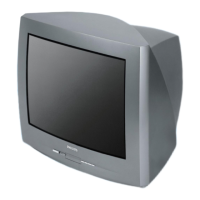
Do you have a question about the Philips 21PT9470/44 and is the answer not in the manual?
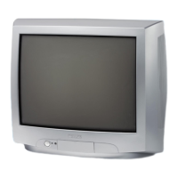
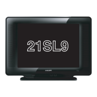
Details product specifications and links for further information.
Provides information on accessing user manuals and support resources.
Explains connection types, color abbreviations, and pinouts.
Refers to block diagrams for PWB/CBA locations.
Outlines essential safety regulations for repair and handling.
Recommends maintenance intervals based on usage conditions.
Highlights critical warnings for preventing damage and ensuring safe operation.
Provides general guidance on measurements, component interchangeability, and symbols.
Lists and defines technical abbreviations used throughout the manual.
Details the step-by-step process for disassembling the TV set.
Outlines the procedures for reassembling the TV set in reverse order.
Specifies conditions for performing measurements during service.
Explains access to Factory Mode for service and alignment.
Indicates that error codes are not applicable for this model.
Provides troubleshooting steps for common TV malfunctions and symptoms.
Sets the conditions required for performing electrical adjustments.
Details the main voltage adjustment procedure using a multimeter.
Guides on entering factory mode and performing software-based alignments.
Lists and explains various parameters adjustable in factory mode.
Provides a general overview of the TV's platform and circuit descriptions.
Describes the function of individual circuits like Tuner, IF, Sound, and Decoder.
Provides block diagram and pin configuration for IC601.
Shows block diagram and pin configuration for IC602.
Details block diagram and pinning information for IC301.
Presents block diagram and pinning information for IC401.
Displays block diagram for the TDA12165 IC (IC101).
Identifies the physical location of various Printed Wiring Boards (PWBs) on the chassis.
Circuit diagram and PWB layout for the power supply unit.
Circuit diagram and PWB layout for the frame deflection circuit.
Circuit diagram and PWB layout for the TV tuner module.
Circuit diagram and PWB layout for the AV switching circuitry.
Circuit diagram and PWB layout for the audio amplifier section.
Circuit diagram and PWB layout for the CPU and decoder functions.
Circuit diagram and PWB layout for the CRT board assembly.
Circuit diagram and PWB layout for the side AV input panel.