Do you have a question about the Philips 22HFL3008D/12 and is the answer not in the manual?
Details on product specifications, available online support, and getting started information.
Information on how to download user manuals and support documentation from Philips websites.
Details on common interface and HDMI digital video/audio input/output connections.
Details on USB, headphone output, TV antenna input, and VGA PC input connectors.
Guidelines for safe repair procedures, including isolation transformers and safety components.
Precautions regarding electrostatic discharge (ESD) and handling components.
General notes on measurements, waveforms, and schematic conventions.
Guidance on deciding whether to exchange or repair a board.
Precautions to avoid electrical shock and ensure safe service operations.
List of abbreviations used in the manual for technical terms and components.
Illustrations and instructions for routing cables within the TV chassis for different models.
Instructions for safely positioning the TV for servicing and measurements.
Procedure for removing the panel and associated components for 32" and 39" models.
Procedure for removing the panel and associated components for 22" and 24" models.
Procedure for removing the panel and associated components for 26" models.
Instructions for re-assembling the TV set after repairs, with notes on cable placement and EMC foams.
Guidance on measuring signals, using test patterns, and controlling diagnostics via ComPair.
Overview of Service Modes (SDM, SAM, Factory, CSM, ComPair) for repair and alignment.
General information applicable to all service modes, including life timer and software identification.
Details on activating and using SDM for predefined settings and measurements.
Instructions for activating and using SAM for NVM modification and alignments.
Overview of Factory mode features like alignments, panel ID, and error buffer clearing.
Purpose and activation of CSM for diagnosing set operation and error codes.
Step-by-step guide to activate Customer Service Mode using remote control sequences.
Diagram illustrating the TV's power states and transitions between them.
Overview of service tools, including ComPair for diagnostics and software upgrades.
Information on upgrading TV software via USB for product improvement.
Procedure to check the current software version before starting an upgrade.
Steps to download the latest software updates from the Philips support website.
Step-by-step guide to update the TV software using a USB memory stick.
Explanation of One-Zip file contents relevant for service operations.
Explanation of error codes used to indicate TV failures and the error buffer.
Methods to read error codes: OSD, blinking LED procedure, or ComPair.
List of available layer 2 error codes and their corresponding defective devices.
Procedure for clearing the error code buffer in SAM, Factory mode, or automatically.
Explanation of how the front LED blinks to indicate errors when OSD is not working.
How the entire error buffer is displayed when Service Mode 'SDM' is entered.
General tips and procedures for fault finding and repair.
Guidance on using the NVM Editor in SAM mode to change NVM contents.
How to upload default NVM values using ComPair for new or corrupted NVMs.
Troubleshooting steps for issues when there is no picture displayed.
Troubleshooting for unstable pictures via HDMI input, checking EDID data.
Troubleshooting for no picture via HDMI input, checking HDCP key validity.
Troubleshooting for TV not starting from stand-by, suggesting software re-flash.
Specific notes on replacing the Class D IC U606 and its powerpad for cooling.
Notes on CSM activation with USB memory stick for dumping CSM content.
Caution regarding volume level when disconnecting speakers to prevent amplifier damage.
Importance of checking Panel Code in CSM after SSB replacement for correct display.
Conditions required for performing electrical adjustments, including power supply and test probes.
Indicates that hardware alignments are not applicable for this chassis.
Procedure for software alignments using SAM mode, focusing on White Point and Display Adjustment.
Steps to perform RGB alignment, setting picture parameters before alignment.
Procedure for adjusting display settings like color temperature and RGB values.
How the microprocessor communicates with I2C ICs using option codes.
Checking and editing option codes within the NVM.
Procedure to check and reset the Display Code for panel types.
Instructions for reloading MAC address after NVM replacement via SAM.
How to identify SSB boards using their 715 code and matching replacement panels.
Rule for defining cable position numbers based on connector numbers and signal flow.
Introduction to the TPM10.1HE LA chassis and its key components like the MTK5580 SCALER.
Lists key components of the chassis including the SCALER, Tuner, and Audio Amplifier.
Reference to chassis block diagrams for detailed architecture understanding.
Diagram showing the layout of components and ICs on the SSB board (top view).
Information on the Power Supply Unit, including replacement procedures and voltage outputs.
Describes the diversity in power supply units based on different display types and backlight technologies.
Details on the on-board DC/DC converters and their respective voltages and current consumptions.
Block diagram of the front-end for the analogue tuner, showing key components.
Block diagram of the front-end for DVB-T/C DTV, listing key components.
Internal block diagram and pin configuration for the LNBH25PQR IC.
Internal block diagram of the MT5580CPOI IC, showing its peripheral functions.
Internal block diagram and pin configuration for the STA381BWTR IC.
Internal block diagram and pin configuration for the MT5136AN IC.
Internal block diagram and pin configuration for the AVL6211LA IC.
Overall block diagram of the 3008 series TV, showing interconnections of major components.
Circuit diagram and power layout for the A 715G5309 Power Supply Unit.
Circuit diagram for the LED driver associated with the A 715G5309 PSU.
Top-side layout diagram for the power supply unit.
Bottom-side layout diagram for the power supply unit.
Circuit diagram for the A 715G5793 Power Supply Unit.
Circuit diagram for the LED driver associated with the A 715G5793 PSU.
Top-side layout diagram for the A 715G5793 PSU.
Bottom-side layout diagram for the A 715G5793 PSU.
Circuit diagram for the A 715G5804 Power Supply Unit.
Circuit diagram for the LED driver associated with the A 715G5804 PSU.
Top-side layout diagram for the A 715G5804 PSU.
Bottom-side layout diagram for the A 715G5804 PSU.
Circuit diagram for the AC input section of the A 715G6050 PSU.
Circuit diagram for the main power stage of the A 715G6050 PSU.
Circuit diagram for the D2D LED driver of the A 715G6050 PSU.
Top-side layout diagram for the A 715G6050 PSU.
Bottom-side layout diagram for the A 715G6050 PSU.
Circuit diagram for the A 380GLP30029DE0 Power Supply Unit.
Layout diagram for the A 380GLP30029DE0 Power Supply Unit.
Circuit diagram for System Power 1 on the B 715G5675 SSB board.
Circuit diagram for System Power 2 on the B 715G5675 SSB board.
Circuit diagram showing peripherals connected to the MTK5580CPOI IC.
Circuit diagram for USB connectors and related components.
Circuit diagram for audio/video input/output and SPDIF connections.
Circuit diagram for the audio amplifier, speaker, and headphone output.
Circuit diagrams for SCART and VGA input connections.
Circuit diagram for LVDS connections and related components.
Circuit diagrams for MII, GPIO, and ServAD interfaces.
Circuit diagrams for T2 Demodulator and CI Card interface.
Circuit diagrams for HDMI switching and connector protection circuits.
Circuit diagrams for DVB T2/C/S2 Tuner, including tuner power and demodulator.
Top-side layout diagram of the SSB board.
Bottom-side layout diagram of the SSB board.
Circuit diagram for the IR/LED panel, including IR receiver and LED driver.
Layout diagrams for the IR/LED board (top and bottom sides).
Circuit diagram for the IR/LED panel, including IR receiver and LED driver.
Layout diagrams for the IR/LED board (top and bottom sides).
Circuit diagram for the keyboard control panel, showing switch and resistor configurations.
Layout diagrams for the keyboard control panel (top and bottom sides).
Circuit diagram for the keyboard control panel, showing switch and resistor configurations.
Layout diagrams for the keyboard control panel (top and bottom sides).
Circuit diagram for the keyboard control panel, showing switch and resistor configurations.
Layout diagrams for the keyboard control panel (top and bottom sides).
Exploded view and parts list for the 22-inch 3008 series TV.
Exploded view and parts list for the 24-inch 3008 series TV.
Exploded view and parts list for the 26-inch 3008 series TV.
Exploded view and parts list for the 32-inch 3008 series TV.
Exploded view and parts list for the 39-inch 3008 series TV.
| Screen Size | 22 inches |
|---|---|
| Resolution | 1920 x 1080 pixels |
| Display Technology | LED |
| Screen shape | Flat |
| Aspect Ratio | 16:9 |
| Contrast ratio (typical) | 1000:1 |
| Response time | 5 ms |
| Brightness | 250 cd/m² |
| HD type | Full HD |
| Supported video modes | 1080p |
| Smart TV | No |
| RMS rated power | 10 W |
| Number of speakers | 2 |
| HDMI Ports | 2 |
| USB 2.0 ports quantity | 1 |
| SCART ports quantity | 1 |
| VESA mounting | Yes |
| VESA mounting interfaces | 100 x 100 mm |
| Product colour | Black |
| Refresh Rate | 60 Hz |
| Weight | 3.5 kg |
| Display diagonal | 55.88 cm |
| Digital signal format system | DVB-T/DVB-C |

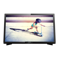
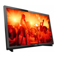

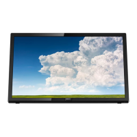

 Loading...