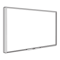
Do you have a question about the Philips 40PFL7007K/12 and is the answer not in the manual?
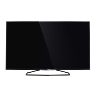
| Screen Size | 40 inches |
|---|---|
| Resolution | 1920 x 1080 pixels |
| Display Type | LED |
| Smart TV | Yes |
| HDMI Ports | 4 |
| USB Ports | 3 |
| Wi-Fi | Yes |
| Ethernet Port | Yes |
| Audio Output | 20 W |
| 3D | No |
| Ambilight | Yes |
| Digital TV Tuner | DVB-T/C/S2 |
| Refresh Rate | 400 Hz Perfect Motion Rate |
Detailed specifications for product support, getting started, manuals, FAQs, and drivers.
Information on where to download user manuals and product information from Philips websites.
Overview of rear and side connectors for various interfaces including SATELLITE and HDMI.
Reference to block diagrams for PWB/CBA locations.
Guidelines for safe repair procedures, including isolation transformer use and safety component replacement.
Important warnings regarding electrostatic discharge (ESD), high voltage, and component replacement.
General notes on measuring voltages/waveforms and schematic conventions.
Details on measuring voltages and waveforms with specific test conditions.
Explains conventions for resistor and capacitor values, and component usage.
Information on consulting the Philips Spare Part web portal for part overviews.
Information on handling BGA devices and temperature profiles.
Rules and tool requirements for lead-free soldering during repair.
Explanation of 'Alternative BOM' as 'Design variant' and its identification via serial number.
Explains how to identify the 14-digit serial number and its components.
Guidance on deciding between board replacement and component-level repair.
Precautions to avoid electrical shock and ensure safe handling of the TV set.
A comprehensive list of abbreviations used in the manual with their meanings.
Illustrates cable routing for 40" 7000/8000 series televisions.
Shows cable dressing for the rear cover of 40" 7000 series TVs.
Illustrates cable routing for the rear cover of 40" 8000 series TVs.
Depicts cable routing for the internal components of 42" 6900 series TVs.
Shows cable routing for the rear cover of 42" 6900 series TVs.
Illustrates cable routing for internal components of 46" 7000/8000 series TVs.
Shows cable routing for the rear cover of 46" 7000 series TVs.
Depicts cable routing for the rear cover of 46" 8000 series TVs.
Shows internal cable routing for 46" 9707 series televisions.
Illustrates cable routing for the rear cover of 46" 9707 series televisions.
Shows internal cable routing for 47" 6900 series televisions.
Depicts cable routing for the rear cover of 47" 6900 series televisions.
Shows internal cable routing for 55" 7000/8000 series televisions.
Illustrates cable routing for the rear cover of 55" 7000 series televisions.
Depicts cable routing for the rear cover of 55" 8000 series televisions.
Shows internal cable routing for 60" 9607 series televisions.
Depicts cable routing for the rear cover of 60" 9607 series televisions.
Recommendations for safe and stable TV placement during servicing.
Step-by-step instructions and warnings for removing the rear cover and SSB.
Step-by-step instructions and warnings for removing the rear cover.
Instructions and visual aids for removing the SSB, including LVDS connector details.
Shows the second part of the SSB LVDS connector catch mechanism.
Illustrates the location and path of the SSB adhesive heat path.
Guidelines for re-assembling the TV set, emphasizing cable placement and EMC foam.
Guidance on using test patterns and measuring signals to identify defective parts.
Introduction to Service Default Mode (SDM), Service Alignment Mode (SAM), and Customer Service Mode (CSM).
Purpose and activation of SDM for pre-defined settings and overriding SW protections.
Default settings for SDM, including picture and sound parameters.
Procedure to activate Service Alignment Mode (SAM) using a remote transmitter.
Details on Hardware Info, Operation hours, Errors, Alignments, Options, and NVM initialization.
Illustrates the location of the display option code sticker on the TV.
Information on SW and HW Events, Test settings, RF4CE pairing, and uploading/downloading to USB.
Instructions on navigating menus within Service Modes using the remote control.
Methods to exit Service Alignment Mode (SAM).
Purpose and activation of CSM for customer support and troubleshooting.
Details on General information (Set type, Production code) and Software versions.
Information on Signal quality, MAC addresses, BDS key, CI module status, and event counters.
Methods to exit Customer Service Mode (CSM).
Explanation of start-up diagrams and their documentation of present supplies.
Visual representation of the TV's state transitions (Off, Standby, Semi Standby, Active, Protection).
Flowchart detailing the process from the 'Off' state to 'Semi Stand-by'.
Continuation of the flowchart illustrating the transition from 'Off' to 'Semi Stand-by'.
Flowchart illustrating the transition from 'Semi Stand-by' to the 'Active' state.
Flowchart illustrating the transition from the 'Active' state back to 'Semi Stand-by'.
Flowchart detailing the transition from 'Semi Stand-by' to the 'Stand-by' state.
Overview of service tools available, including ComPair.
Introduction to ComPair, its features, specifications, and connection instructions.
Explanation of the error code buffer, its logging mechanism, and error types.
Explanation of the error code buffer, its logging mechanism, and error types.
Methods for reading error codes from the buffer, including on-screen display and blinking LED procedures.
Methods for clearing the error buffer, either via SAM menu or automatic reset.
Details on the error buffer contents, fault detection mechanisms, and interpretation of errors.
Information on rebooting, specific error codes, and their causes.
Explanation of Layer 1 and Layer 2 blinking LED procedures for error diagnosis.
Explanation of Layer 1 and Layer 2 blinking LED procedures for error diagnosis.
Note that no error codes are displayed if the error buffer is empty.
Example of how Layer 2 error codes are displayed via blinking LED.
Methods to activate CSM for Layer 1 errors and SDM for Layer 2 errors.
Overview of software-based protections related to supplies and safety mechanisms.
Overview of software-based protections related to supplies and safety mechanisms.
How supply dips affect the set, leading to cold reboots or protection.
Monitoring of voltages and IC observers during start-up to detect malfunctions.
Guidance on fault finding and repair strategies.
Information on fine-tuning spare Ambilight modules or recovering original settings.
How CSM activation aids in concluding that the operating system is working.
Detailed description of the DC/DC converters, their input voltages, and output specifications.
Tips for finding failures in DC/DC converters by checking start-up sequences.
General debugging tips, including behavior comparison and fuse checking.
Reference to section 7.2.1 for fault finding tips on the power supply unit.
Procedure to exit the factory mode using specific buttons.
How to use Hyperterminal and ComPair for logging TV startup and reboot events.
Possible cases and interpretations of UART loggings, including error codes.
Caution regarding disconnecting speakers while the TV is on.
Recommendations for checking LED drivers when there is no picture or backlight.
Importance of checking and programming the correct display option code, especially after SSB replacement.
Flowchart and instructions for exchanging an SSB, including important attention points.
Detailed step-by-step guide for SSB replacement with advice and remarks.
Visual guide highlighting friction traces and damaged components.
Visual guide showing mounting attention points for SSB fixation.
A step-by-step flowchart for the SSB replacement procedure.
Flowchart for disabling Factory mode after SSB replacement.
Information on software storage (NAND Flash) and user upgrades via USB.
Note regarding security keys (CI+, MAC address) requiring a new SSB.
Steps to perform after SSB replacement, including option numbers, software updates, and alignments.
Instructions for automatic and manual software upgrades via USB.
Note regarding potential issues with 'autorun.upg' recognition during manual download.
Steps for handling the 'Back-up Software Upgrade Application' if the default fails.
Procedure to start the back-up software upgrade application manually.
Method for upgrading standby software via USB, similar to main software upgrades.
Explanation of the contents and usage of one-zip software files for different components.
Reference to UART logging procedures for fault finding.
Conditions required for performing electrical adjustments, including power supply and warm-up time.
Steps for setting correct options in SAM and storing them.
Indicates that hardware alignments are not applicable.
Procedures for aligning white point and Ambilight using SAM.
Detailed steps for aligning white point using SAM, with and without a color analyzer.
Alignment values for white D using Minolta CA-210.
Alignment values for white D using Minolta CS-200.
Default white tone settings for 40" models.
Default white tone settings for 42" models.
Default white tone settings for 46" models.
Default white tone settings for 46" models.
Default white tone settings for 47" models.
Default white tone settings for 55" models.
Default white tone settings for 60" models.
Procedure for aligning Ambilight modules by matrix and brightness.
Table showing matrix correction values for Ambilight modules.
Indicates TCON alignment is not applicable.
Information on setting microprocessor options for communication with ICs.
Explanation of microprocessor communication with I2C ICs and option code setting.
How to change options using option codes from 2011 onwards.
How to set option numbers using two long strings found on the TV's rearcover sticker.
Reference to the rearcover sticker for correct option codes.
Note about pressing OK after editing option numbers.
Crucial step of resetting NVM on a repaired SSB with default service values.
Setting type number, production code, and 12NCs after SSB replacement.
How to identify the correct ordering number (12nc) of a new SSB from its sticker.
Illustration showing how to identify the SSB ordering number.
Summary of SAM modes and their functionalities.
Table summarizing SAM main menu, sub-menus, and descriptions.
Overview of the QFU1.1E LA chassis and its place in the FUSION platform.
Details about chassis block diagrams and an overview of the FUSION 2012 architecture.
Block diagram illustrating the FUSION platform architecture for specific TV ranges.
Block diagram illustrating the FUSION platform architecture for 9xxx range televisions.
Top view of the SSB showing the layout of various components and connections.
Visual representation of the SSB layout with components identified.
Bottom view of the SSB showing the layout of components like FPGA, CA-side, SDM, and Set NVM.
Information about the power supply unit as a service black box.
Details on ordering replacement boards and replacing fuses.
Reference to figures 7-5 and 7-6 for power architecture and figure 7-7 for start-up steps.
Block diagram showing the general power architecture of the chassis.
Diagram illustrating the functional supply overview of the chassis.
Reference to figures 7-8 to 7-11 for configuration details.
Flowchart showing the functional power overview and sequence.
Block diagram of the back-end configuration for xxPFL6xxx/xx series.
Block diagram of the back-end configuration for xxPFL7xxx/xx and xxPFL8xxx/xx series.
Block diagram of the back-end configuration for xxPFL9xxx/xx series.
Block diagram of the back-end configuration for Platinum (Cinema) series.
Internal block diagram and pin configuration of the Tuner-channel decoder IC.
Wiring diagram for 7000 series, 2-sided AmbiLight 40" televisions.
Wiring diagram for 8000 series, 3-sided AmbiLight 40" televisions.
Wiring diagram for 6000 series, 2-sided AmbiLight 42" televisions.
Wiring diagram for 7000 series, 2-sided AmbiLight 46" televisions.
Wiring diagram for 8000 series, 3-sided AmbiLight 46" televisions.
Wiring diagram for 9000 series, 3-sided AmbiLight 46" televisions.
Wiring diagram for 6000 series, 2-sided AmbiLight 47" televisions.
Wiring diagram for 7000 series, 2-sided AmbiLight 55" televisions.
Wiring diagram for 8000 series, 3-sided AmbiLight 55" televisions.
Wiring diagram for 9000 series, 3-sided AmbiLight 60" televisions.
Block diagram illustrating video signal flow and component connections.
Block diagram illustrating audio signal paths and component connections.
Diagram showing control and clock signal interconnections between major components.
Diagram illustrating I2C communication paths between various ICs.
Overview of the different power supply lines distributed across various boards.
Circuit diagrams and PWB layouts for the B 310431365554 series.
Circuit diagram for the B01A board, showing connectors and protection circuits.
Circuit diagram for the B01B board, detailing the Fusion supply and DC/DC converters.
Circuit diagram for the B01C board, showing DVBS supply and DC/DC converters.
Circuit diagram for the B01D board, illustrating power sequencing DC/DC converters.
Page is intentionally blank.
Circuit diagram for the B01E board, showing miscellaneous components and connections.
Circuit diagram for the B02A board, detailing the Tuner and Channel Decoder.
Circuit diagram for the B02B board, showing the DVBS Front-end and diversity matrix.
LVDS fanout diagram for the B03A board, showing connections to the Fusion SoC.
Circuit diagram for the B03B board, detailing the UMAC controller and DDR3 memory interface.
Circuit diagram showing the UMAC 1 DDR3 memory interface connections.
Circuit diagram showing the UMAC 0 DDR3 memory interface connections.
LVDS fanout diagram for DDR memory connections on the B03E board.
Circuit diagram for the Fusion power supply, showing various voltage regulators.
Circuit diagram for the control board (B04A), showing I2C and other control signals.
Circuit diagram for the V-by-One output interface on the B04B board.
Circuit diagram for the V-disp output on the B04C board, including VDISP-SWITCH.
Circuit diagram showing the connector and circuitry for the backlight control.
Circuit diagram related to tuner CVBS debugging.
Circuit diagram showing audio and video input/output connections.
Circuit diagram for the EMMC controller.
Circuit diagrams for the second source DC-DC converters.
Circuit diagram related to IR debug.
Circuit diagram for the Class-D audio amplifier.
Circuit diagram for analogue external connections.
Circuit diagram for the HDMI connectors and associated components.
Circuit diagram for the HDMI-ARC (Audio Return Channel) functionality.
Circuit diagram for the USB ports and controller.
Circuit diagram for the service connector and related components.
Circuit diagram for the Ethernet interface.
Circuit diagram for the NAND Flash and EEPROM memory.
Circuit diagram for analogue external interfaces.
Circuit diagrams for DC-DC converters.
Circuit diagram for DC-DC converters, specifically for +3V3 and +1V2-FA output.
Page is intentionally blank.
Circuit diagram for the audio output section.
Circuit diagram for the conditional access module interface.
Circuit diagram for the Front-End (FE) section.
Circuit diagram for the serial flash memory.
Circuit diagram showing peripherals connected to the Fusion SoC.
Circuit diagram for the HDMI interface.
Circuit diagram for the control logic, showing I2C communication.
Circuit diagram for the temperature sensor.
Circuit diagram showing strap options for configuration.
Circuit diagram for the LPC debug interface.
Circuit diagram for the headphone output circuitry.
Circuit diagram for the internal USB hub and ports.
Circuit diagram for the common interface (CI) slot.
Circuit diagram showing power and control connections for the FPGA.
Diagram illustrating FPGA I/O banks and their pin assignments.
Circuit diagram for the CPLD (Complex Programmable Logic Device).
Circuit diagram for the AmbiLight LED control circuitry.
Circuit diagram showing interconnects between components.
Top layout view of the SSB board, showing placement of components.
Bottom layout view of the SSB board, showing component placement.
Circuit diagram for the B01A board, showing connectors and protection circuits.
Circuit diagram for the Fusion supply DC/DC converters.
Circuit diagram for the DVBS supply DC/DC converters.
Circuit diagram for the power sequencing DC/DC converters.
Page is intentionally blank.
Circuit diagram for the B01E board, showing miscellaneous components and connections.
Circuit diagram for the Tuner and Channel Decoder.
Circuit diagram for the DVBS Front-end.
LVDS fanout diagram for the B03A board, showing connections to the Fusion SoC.
Circuit diagram for the UMAC controller and DDR3 interface.
Circuit diagram for UMAC 1 DDR3 memory interface.
Circuit diagram for UMAC 0 DDR3 memory interface.
LVDS fanout diagram for DDR memory connections on the B03E board.
Circuit diagram for the Fusion power supply fanout.
Circuit diagram for the control board, showing I2C and other control signals.
Circuit diagram for the LVDS output interface on the B04B board.
Circuit diagram for the V-disp output on the B04C board.
Circuit diagram for the backlight connector and associated circuitry.
Circuit diagram related to tuner CVBS debugging.
Circuit diagram showing audio and video connections.
Circuit diagram for the EMMC controller.
Circuit diagrams for second source DC-DC converters.
Circuit diagram related to IR debug.
Circuit diagram for the Class-D audio amplifier.
Circuit diagram for analogue external connections.
Circuit diagram for the HDMI connectors and associated components.
Circuit diagram for the HDMI-ARC (Audio Return Channel) functionality.
Circuit diagram for the USB ports and controller.
Circuit diagram for the service connector and related components.
Circuit diagram for the Ethernet interface.
Circuit diagram for the NAND Flash and EEPROM memory.
Circuit diagram for analogue external interfaces.
Circuit diagrams for DC-DC converters.
Circuit diagram for DC-DC converters, specifically for +3V3 and +1V2-FA output.
Circuit diagram for the audio output section.
Circuit diagram for the conditional access module interface.
Circuit diagram for the Front-End (FE) section.
Circuit diagram for the serial flash memory.
Circuit diagram showing peripherals connected to the Fusion SoC.
Circuit diagram for the HDMI interface.
Circuit diagram for the control logic, showing I2C communication.
Circuit diagram for the temperature sensor.
Circuit diagram showing strap options for configuration.
Circuit diagram for the LPC debug interface.
Circuit diagram for the headphone output circuitry.
Circuit diagram for the internal USB hub and ports.
Circuit diagram for the common interface (CI) slot.
Circuit diagram showing power and control connections for the FPGA.
Diagram illustrating FPGA I/O banks and their pin assignments.
Circuit diagram for the CPLD (Complex Programmable Logic Device).
Circuit diagram for the AmbiLight LED control circuitry.
Circuit diagram showing interconnects between components.
Top layout view of the SSB board, showing placement of components.
Bottom layout view of the SSB board, showing component placement.
Circuit diagrams and PWB layouts for keyboard modules.
Circuit diagram for the keyboard control panel.
Circuit diagrams and PWB layouts for keyboard control modules.
Circuit diagram for the keyboard control module.
Layout diagrams (top and bottom) for the keyboard control module.
Circuit diagrams and PWB layouts for keyboard control modules.
Circuit diagram for the touch and proximity local keyboard control module.
Circuit diagrams and PWB layouts for sensor boards.
Circuit diagram for the sensor board, including IR, LED, RF, and light sensors.
Layout diagrams (top and bottom) for the sensor board.
Circuit diagrams and PWB layouts for sensor boards.
Circuit diagram for the sensor board with IR, LED, RF, and light sensor components.
Layout diagrams (top and bottom) for the sensor board.
Circuit diagrams and PWB layouts for AmbiLight modules.
Circuit diagram for AL1 AmbiLight module with 16 LEDs.
Circuit diagram for AL2 AmbiLight module with 16 LEDs.
Circuit diagram for AL3 AmbiLight module with 16 LEDs.
Circuit diagrams and PWB layouts for AmbiLight modules.
Circuit diagram for AL1 AmbiLight module with 13 LEDs.
Circuit diagram for AL2 AmbiLight module with 13 LEDs.
Circuit diagram for AL3 AmbiLight module with 13 LEDs.
Circuit diagram for AL2 AmbiLight module with 13 LEDs.
Circuit diagram for AL3 AmbiLight module with 13 LEDs.
Circuit diagrams and PWB layouts for AmbiLight modules.
Circuit diagram for AL1 AmbiLight module with 16 Everlight LEDs.
Circuit diagram for AL2 AmbiLight module with 16 Everlight LEDs.
Circuit diagram for AL3 AmbiLight module with 16 Everlight LEDs.
Circuit diagrams and PWB layouts for AmbiLight modules.
Circuit diagram for AL1 AmbiLight module with 9 Everlight LEDs.
Circuit diagram for AL2 AmbiLight module with 9 Everlight LEDs.
Circuit diagrams and PWB layouts for AmbiLight modules.
Circuit diagram for AL1 AmbiLight module with 15 LEDs.
Circuit diagram for AL2 AmbiLight module with 15 LEDs.
Circuit diagram for AL3 AmbiLight module with 15 LEDs.
Circuit diagram for AL1 AmbiLight module with 16 Everlight LEDs.
Circuit diagram for AL2 AmbiLight module with 16 Everlight LEDs.
Circuit diagram for AL3 AmbiLight module with 16 Everlight LEDs.
Circuit diagrams and PWB layouts for AmbiLight modules.
Circuit diagram for AL1 AmbiLight module with 15 Everlight LEDs.
Circuit diagram for AL2 AmbiLight module with 15 Everlight LEDs.
Circuit diagram for AL3 AmbiLight module with 15 Everlight LEDs.
Circuit diagrams and PWB layouts for AmbiLight modules.
Circuit diagram for AL1 AmbiLight module with 12 Everlight LEDs.
Circuit diagram for AL2 AmbiLight module with 12 Everlight LEDs.
Circuit diagrams and PWB layouts for AmbiLight modules.
Circuit diagram for AL1 AmbiLight module with 10 Everlight LEDs.
Circuit diagram for AL2 AmbiLight module with 10 Everlight LEDs.
Circuit diagram for AL3 AmbiLight module with 10 Everlight LEDs.
Circuit diagrams and PWB layouts for AmbiLight modules.
Circuit diagram for AL1 AmbiLight module with 9 Everlight LEDs.
Circuit diagram for AL2 AmbiLight module with 9 Everlight LEDs.
Circuit diagrams and PWB layouts for AmbiLight modules.
Circuit diagram for AL1 AmbiLight module with 7 Everlight LEDs.
Circuit diagram for AL2 AmbiLight module with 7 Everlight LEDs.
Exploded view and parts list for 7000 series 40" televisions.
Exploded view and parts list for 8000 series 40" televisions.
Styling information for 6000 series 42" televisions, noted as not available.
Exploded view and parts list for 7000 series 46" televisions.
Exploded view and parts list for 8000 series 46" televisions.
Styling information for 9000 series 60" televisions, noted as not available.
Styling information for 6000 series 47" televisions, noted as not available.
Exploded view and parts list for 7000 series 55" televisions.
Exploded view and parts list for 8000 series 55" televisions.
Styling information for 9000 series 60" televisions, noted as not available.