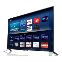
Do you have a question about the Philips 55PFL7008K/12 and is the answer not in the manual?
Details on product support, information, getting started, manuals, FAQs, software & drivers.
Details on side and rear connections for various inputs and outputs.
Safety regulations and procedures to follow during and after repairs.
Important notes regarding schematics, spare parts, BGA IC handling, and lead-free soldering practices.
Alphabetical list of abbreviations used in the manual with their meanings.
Guidance on how to route and secure internal cables within the set.
Recommended positions for the TV set during servicing to ensure safety and prevent damage.
Instructions for the removal of assemblies and panels from the TV set.
Procedures for reassembling the TV set, emphasizing correct cable placement and EMC foam mounting.
Key test points and conditions for measurements, utilizing test patterns.
Explanation of Service Default Mode (SDM) and Service Alignment Mode (SAM) for technician use.
Diagrams illustrating the TV set's start-up process under various conditions.
Information on service tools, including ComPair, and procedures for memory tests.
Details on error codes, their meaning, and how they are displayed.
Procedure for identifying errors via the blinking LED on the front panel.
Explanation of software protections and fault conditions that trigger them.
Guidelines for diagnosing failures in power conversion, distribution, and debugging.
Procedures for upgrading main and standby software via USB.
Conditions and requirements for performing electrical alignments, including power supply and measurement probes.
Procedure for white point alignment, including picture settings and analyser usage.
Step-by-step procedure for setting correct options and performing alignments in SAM mode.
Information on setting microprocessor communication and option numbers.
Procedure for resetting the NVM on a repaired SSB and setting service parameters.
Guidance on identifying the correct ordering number (12nc) for an SSB.
Overview of all available Service Alignment Mode (SAM) functions.
Overview of the FUSION 2013 architecture, referring to block diagrams.
Block diagram and pinning information for the DVBT2 channel decoder IC.
Circuit diagram and PWB layout for the SSB (310431366124).
Circuit diagram and PWB layout for the USB internal module B01D.
Circuit diagram and PWB layout for the Hybrid T/C tuner module B02A.
Circuit diagram and PWB layout for the Satellite tuner module B02B.
Circuit diagram and PWB layout for the DVBT2 channel decoder module B02C.
Circuit diagram and PWB layout for the DVBS/S2 channel decoder module B02D.
Circuit diagram and PWB layout for the Fusion module B03A.
Circuit diagram and PWB layout for the Fusion Umac controller module B03B.
Circuit diagram and PWB layout for the Umac 1 DDR3 module B03C.
Circuit diagram and PWB layout for the Umac 0 DDR3 module B03D.
Circuit diagram and PWB layout for the Fusion module B03E.
Circuit diagram and PWB layout for the Fusion power supply module B03F.
Circuit diagram and PWB layout for the Control module B04A.
Circuit diagram and PWB layout for the LVDS module B04B.
Circuit diagram and PWB layout for the Output Vdisp module B04C.
Circuit diagram and PWB layout for the Audio - video module B04E.
Circuit diagram and PWB layout for the Fusion supply module B04F.
Circuit diagram and PWB layout for the Backlight microcontroller module B04G.
Circuit diagram and PWB layout for the eMMC module B04H.
Circuit diagram and PWB layout for the Class-D amplifier module B05A.
Circuit diagram and PWB layout for the Sensor board and AmbiLight module B05C.
Circuit diagram and PWB layout for the HDMI module B06A.
Circuit diagram and PWB layout for the HDMI-ARC module B06B.
Circuit diagram and PWB layout for the Ethernet module B06D.
Circuit diagram and PWB layout for NAND flash, serial flash, and EEPROM.
Circuit diagram and PWB layout for the DC-DC converter module B06G.
Circuit diagram and PWB layout for the DC-DC converter module B06H.
Circuit diagram and PWB layout for the CI conditional access module B06I.
Circuit diagram and PWB layout for the FE (Front End) module B06J.
Circuit diagram and PWB layout for the HDMI module B06K.
Circuit diagram and PWB layout for the Control, temperature sensor, and service module B06L.
Circuit diagram and PWB layout for the Strap options module B06M.
| Screen Size | 55 inches |
|---|---|
| Display Type | LED |
| Smart TV | Yes |
| HDMI Ports | 4 |
| USB Ports | 3 |
| Wi-Fi | Yes |
| Ethernet Port | Yes |
| Audio Output | 20 W |
| Refresh Rate | 400 Hz |
| Energy Class | A+ |
| Resolution | 1920 x 1080 pixels (Full HD) |
| 3D | Yes (Active 3D) |
| Ambilight | Yes |
| Digital TV Tuner | DVB-T/C/S/S2 |
| Connectivity | Wi-Fi, Ethernet |


 Loading...