EasyManua.ls Logo

Philips FW-V787/21M User Manual

Philips FW-V787/21M
92 pages
To Next Page IconTo Next Page
Page #1 background imageLoading...
Page #1 background image
GB
CLASS 1
LASER PRODUCT
Service
Service
Service
Service
Service
FW-V787/21M
TABLE OF CONTENTS
Page
Location of pc boards & Version variations................1-2
Technical Specifications .............................................1-3
Measurement setup ....................................................1-4
Service Aids, Safety Instruction, etc...........................1-5
Preparations & Controls .............................................1-7
Disassembly Instructions & Service positions .............. 2
Service Test Programs ...............................................3-1
Set Block diagram ......................................................4-1
Set Wiring diagram .....................................................4-2
Front Control Board ....................................................... 5
Front Display Board ....................................................... 6
ECO6 Tuner Board : Systems Non-Cenelec.............. 7A
VCD-MPEG-01B Module ............................................... 8
ETF7 ND Tape Module .................................................. 9
3CDC-LC-VCD Module ...............................................10
P2002 100W VCD Module .......................................... 11
Center/Surround & Matrix Surround Socket Board...11A
AF9 Board.................................................................... 12
VCD GND Isolator Board ............................................ 13
Set Mechanical Exploded view & parts list ................. 14
©
Copyright 2002 Philips Consumer Electronics B.V. Eindhoven, The Netherlands
All rights reserved. No part of this publication may be reproduced, stored in a retrieval system or
transmitted, in any form or by any means, electronic, mechanical, photocopying, or otherwise
without the prior permission of Philips.
Published by SL 0307 Service Audio Printed in The Netherlands Subject to modification
Mini System
3140 785 32420
Version 1.0
VIDEO CD
Service Manual

Table of Contents

Question and Answer IconNeed help?

Do you have a question about the Philips FW-V787/21M and is the answer not in the manual?

Philips FW-V787/21M Specifications

General IconGeneral
BrandPhilips
ModelFW-V787/21M
CategoryStereo System
LanguageEnglish

Summary

Specifications

Video CD Specifications

Specifications for video CD audio and video performance.

Amplifier Specifications

Specifications for output power, frequency response, and input sensitivity.

Service Aids and Component Handling

ESD and Safety Precautions

General ESD Protection Guidelines

Warnings and precautions regarding electrostatic discharge (ESD) during repair.

Laser Product Safety Warnings

Warnings about invisible laser radiation when the product is open.

Safety Regulations and Part Usage

Requirements for restoring the set to original condition and using specified parts.

Leakage Current Test Procedure

Test procedure to ensure safety after servicing.

Maintenance and Troubleshooting

Disc Player Error Solutions

Troubleshooting for "UNREADABLE DISC" and "NO DISC" errors.

Video and TV System Troubleshooting

Solutions for video output and TV system setting issues.

System Response and Audio Quality Problems

Solutions for unresponsiveness, poor audio, and reversed outputs.

Dismantling Instructions

CDC Module and Front Panel Disassembly

Procedures for dismantling the CDC module and front panel.

Separating MPEG and CDC Modules

Method to separate the MPEG and CDC modules from each other.

Component Board Dismantling and Repair Hints

Front Display and Control Board Dismantling

Steps to dismantle front display and control boards.

Rear Portion Board Dismantling

Steps to dismantle boards located in the rear section of the unit.

ETF Tape Module Dismantling

Steps to dismantle the ETF tape module.

Repair Hints

Flex Cable Handling Precautions

Precautions for handling delicate flex cables to prevent damage.

Service Test Program

Tuner Test Procedures

Steps and expected results for testing the tuner function.

Quartz and Display Test

Procedures for testing quartz oscillator and system display elements.

VCD Test Routines

Detailed test routines for VCD functions including servo and disc tests.

Set Block Diagram

Set Wiring Diagram

AF9/AF10 Board Wiring

Wiring connections for the AF9/AF10 board.

L/R Amplifier & Supply Board Wiring

Wiring connections for the L/R amplifier and supply board.

Tuner Board Wiring

Wiring connections for the tuner board.

Front Board Wiring

Wiring connections for the front control and display boards.

Rear Portion Wiring Diagram

Wiring connections for rear boards like video out.

Front Control Board Details

Front Control Board Layouts

Component and chip layouts for the front control board.

Front Control Board Circuit Diagram

Circuit diagram for the front control board.

Front Control Board Layouts

Front Control Board Circuit Diagram

Front Display Board Details

Front Display Board Layouts

Chip and component layouts for the front display board.

Front Display Board Circuit Diagram

Circuit diagram for the front display board.

Front Display Board Chip Layout

Front Display Board Component Layout

Front Display Board Circuit Diagram

ECO6 Tuner Board

ECO6 Tuner Board Block Diagram

Block diagram illustrating the functional blocks of the tuner board.

ECO6 Tuner Board Schematics and Layouts

Schematic diagram, component layout, and adjustment table.

TUNER BOARD ECO6 Systems Layouts

Componentside View

Component layout of the tuner board from the components side.

Copperside View

Component layout of the tuner board from the copper trace side.

TUNER ADJUSTMENT TABLE

Varicap Alignment Procedures

Procedures for adjusting varicap alignment for FM, MW, and LW bands.

VCD - MPEG-01B MODULE

MPEG Module Introduction and Block Diagram

Overview of the MPEG module and its main block diagram.

Brief Introduction on the MPEG Module

MPEG-01B Block Diagram

8-BIT MICROCONTROLLER (IC 7212) Internal Block Diagram

ES3880 Video CD Processor Chip

ES3880 Pin Descriptions

Detailed description of each pin on the ES3880 Video CD Processor chip.

Visba Video CD PC Block Diagram

Block diagram illustrating the Visba Video CD PC processor.

ES3883 Video CD Companion Chip

ES3883 Pin Descriptions

Detailed description of each pin on the ES3883 Video CD Companion chip.

MPEG-01B Board Layout

ES3880 Circuit Diagram

ES3883 Circuit Diagram

Audio Circuit Diagram

ETF7 TAPE MODULE

ETF7 Tape Module Overview

Includes block diagram, introduction, connector assignments, and adjustments.

Tape Mechanism Block Diagram

Tape Mechanism Function Descriptions

Dolby Circuitry and Level Settings

Description of Dolby noise reduction circuit and level adjustment procedures.

Connector Assignments

Tape Mechanism Electronics

Tape Adjustment and Check Procedures

Table detailing procedures for adjusting motor speed, wow/flutter, azimuth, and frequency response.

Tape Mechanism Layouts

Analog Circuit Diagram

Servo Control Circuit Diagram

3CDC-LC-VCD MODULE

CD Changer Wiring and Block Diagrams

Wiring and block diagrams for the CD changer module.

CD Changer Service Hints

CD Mechanism Replacement Precautions

Cautionary notes on ESD and power supply for CD mechanism replacement.

CD Mechanism Replacement Procedure

Step-by-step instructions for replacing the CD mechanism.

Laser Diode Protection Note

Important note regarding laser diode protection and solder joint removal.

CD Changer Service Hints

CD Changer Wiring

BLOCK DIAGRAM 3CDC-LC VCD Version

Mainboard Block Diagram

Block diagram illustrating the mainboard, CD mechanism, and signal processor.

3CDC-LC (Herman) Copperside View

3CDC-LC Components Seen from Copperside

3CDC-LC Circuit Diagram Part 1

Signal Processor and Microcontroller Interface

Interface between the signal processor and the microcontroller.

3CDC-LC Circuit Diagram Part 2

3CDC-LC Circuit Diagram Part 3

EXPLODED VIEW (3CDC-LC MODULE)

P2002 100W VCD MODULE

P2002 Module Wiring Diagram

Wiring diagram for the P2002 100W VCD module.

Mains Board Component View

Mains Socket Views and Diagram

MAINS BOARD - CIRCUIT DIAGRAM

LEFT/RIGHT AMPLIFIER & SUPPLY BOARD - COMPONENT VIEW

LEFT/RIGHT AMPLIFIER & SUPPLY BOARD - CIRCUIT DIAGRAM (PART 1)

LEFT/RIGHT AMPLIFIER & SUPPLY BOARD - CIRCUIT DIAGRAM (PART 2)

CENTER/SURROUND & MATRIX SURROUND SOCKET BOARD

Center/Surround & Matrix Surround Socket Diagrams

AF9 BOARD

AF9 Board Introduction and Features

Overview of AF9 board features like IC functions, mixing, and outputs.

AF9 BOARD LAYOUTS

Component Layout

Component placement diagram for the AF9 board.

Chip Layout

Chip placement diagram for the AF9 board.
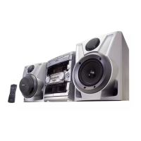
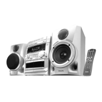
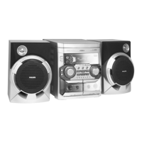
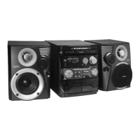
AF9 BOARD CHIP LAYOUT

AF9 BOARD CIRCUIT DIAGRAM (PART 1)

AF9 BOARD CIRCUIT DIAGRAM (PART 2)

AF9 BOARD CIRCUIT DIAGRAM (PART 3)

VCD GND ISOLATOR BOARD

VCD GND ISOLATOR BOARD - CIRCUIT DIAGRAM

SET MECHANICAL EXPLODED VIEW

MECHANICAL & ACCESSORIES PARTS LIST - MAIN UNIT

Related product manuals