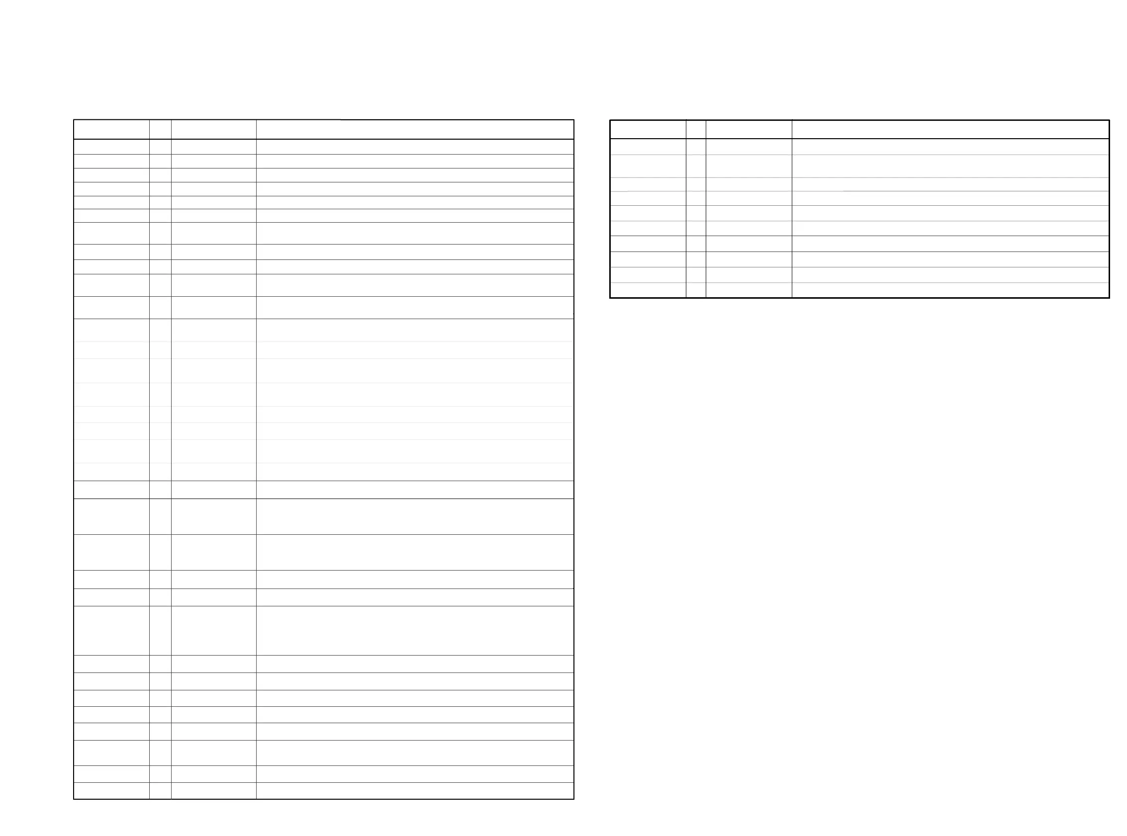
VCC5OP,VCC5IP
VCCKP
This pin supplies 3.3 volts to inter
nal logic.
GNDIKP
Ground for internal logic and input p
ad.
VCCAP
This pin supplies 3.3 volts to internal PLL circuit.
GNDAP
This pin is the ground for internal PLL circuit.
VCCTVP
This pin supplies 3.3 volts or 5 volts to TV encoder
associated interface signals.
GNDTVP
This pin is ground for TV encoder associated interface
signals.
CLKIN, CLKIO
These two pins con
nect to 27 MHz crystal.
TEST_MODE
Bringing this pin high will put the chip in test mode.
This pin should
norm
ally be low.
BIST_MODE
Bringing this pin
high
will put the chip in bist test mode.
This pin should normally be low.
RESET_B
This signal is active low and must be active for at least
25 CLK27OUT clock
cycles. After reset, the
SPCA702A will be in the initialization state.
I
I
102
CD_DATA
This pin is inp
ut for ser
ial data from CD-DSP.
CD_LRCK
CD_LRCK provides 16-b
it w
ord synchronization to the
SPCA702A and
has
several programmable features,
such as polarity, delay and pulse mode.
CD_BCK
The CD_BCK is the CD-Decoder bit clock. The
SPCA702A can
accept multiple BCK rates.
AUD_DATA
This pin is used
as the serial audio data clocked
out
relative to AUD_BCK.
AUD_EMP
This signal is used to
control the de-emphasis
circuitry
of the audio output
DACs. In CD-DA pass-through
mode, this output follows the state of
the CD_EM
P
signal; when in VCD mode, this pin follows the LSB of
the emphasis field of the MPEG-1 audio header.
HSYNC_IN
Horizontal sync signal input from TV encoder.
VSYNC_IN
Vertical sync signal input from TV encoder.
DATA_TV(7:0)
These pins form the video data output bus. It contains
multiplexed Luminance and Chrominance video data.
PAL_NTSC
This pin controls the PAL/NTSC mode of TV encoder.
CLK27OUT
27 MHz video pixel clock output to the TV encoder.
DA(11:0
)
Address bus of fast-page or EDO DRAM
DD(15:0)
DRAM access data bus. The direction is determined
by DR_WE_L signal.
CAS_B
DRAM CAS signals.
RAS_B
DRAM RAS signals for bank 1 to 0.
WE_B
DRAM
write enable signal.
NDATA(7:0)
Bus interface between host and Mpeg chip.
NSTROBE
Strobe signal for other host interface signals
NWRITE
write/read enable
AUD_XCK
When the CA700A is programmed for external audio
clock mode,
the audio clock will come from this signal.
When programmed for internal
audio clock, this signal will
reflect the internal audio clock.
AUD_BCK
This pin is the audio bit cloc k output. Depending on
audio output mode,
this signal can be derived from the master clock or be AUD_XCK divided
by 8. It can be either 48 or 32 times the sampling clock.
AUD_LRCK
This pin is used as the Left/Right data channel indicator.
O
O
O
O
O
O
O
Name
I/O
Pin Description
I
I
I
I
I
I
I
O
O
O
This pin supplies 5 volts to I/O pad.
GND5OP
Ground for I/O buffers.
I/O
I
I
I
I
I
I
I
O
I
I
I/O
I/O
I/O
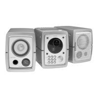
3,29,42,58,79,107
6,31,44,60,80,109
34,46,68,104,127
35,70,128
7
9
97
99
4-5
8
10
103
101
100
86
87
96-89
98
88
81
85
84
83
82
48-47,45,43,41-36
12-19,27-20
30
32-33
28
105-106,108,
110-114
115
118