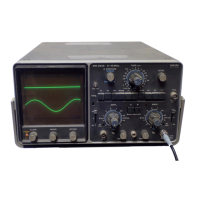
114
The
operation
of
the main
time-base
generator
is
based
on the principle
that
a capacitor
charges
linearly
when
a constant-current
source is
applied,
and
can be
periodically
discharged
rapidly
by means
of an
electronic
switch.
In
this
way,
a linear
saw-tooth
waveform
is
generated.
The
constant-current
source
consists
of
transistors V913,
V914 and
integrated
circuit
D903.
The
emitter
voltage
of
V914
has
the
same
potential
as point
3
of
D903,
therefore
a constant
voltage
exists
across
the series
circuit
of R926
and the
charging
resistors
on switch
TIME/DIV
SI 5.
This
voltage,
and thus
the
charging
current
may
be
varied
by
means of
potentiometer R1
1
and
the
preset potentiometers
R91
1 and R913,
which
compensate
for
the
tolerances
of the
timing
capacitors.
In
the
TRIG,
position V931
is
switched off
because
of
the
+5.2 V
applied
to its base
by switch
S8
(AUTO).
If
point 1
4 of
the
master
slave flip-flop
D901
is
logic "high"
due to
a trigger
pulse,
V929
will
also
be
switched
off.
Consequently,
its
collector
will
be negative
and
switching
transistors
V906,
V907
will be
turned
off
(discharge
switch
open) and
the timing
capacitors
C91
6
and
C91 7 in
parallel
(and C91
2,
C91
3 or
C91
4 as selected)
will
be
charged.
This
charging
voltage
is
applied
via the
buffer
stage
consisting
of the
Darlington
pair emitter-
follower
V922,
V923
(h.f.
path)
and
via the
operational
amplifier D904
together
with
V924
(l.f.
path)
to
point
1 2 of
the R;
S; flip-flop
D902.
This
flip-flop
reaches
its switching
voltage
when
the
time-base-saw-tooth
voltage
rises
to
approximately
-(-4,3
V.
Output
14
will then
be "high"
and
output
15 will
be "low".
Since
the
collector
of
V937 is
positive
(see
operation
of AUTO
circuit),
diodes
V927
and V926
will
conduct
and
the
"high"
output
on
point
14 of
D902
will
be
applied
to point
12 (S input)
of flip-flop
D901.
This
results in
a
"low"
output
on
point 14
of D901
irrespective
of the
state of the
other
inputs. The
"low"
output
causes
V929
to start
conducting
and its
collector
becomes less
negative.
Consequently,
switching
transistors
V906,
V907
conduct
(discharge
switches
closed),
the
timing
capacitance
is
discharged
and
point 1
2
of D902
drops
below
the
switching
level.
Transistor
V944,the
base of which
was
turned
on by
the "high"
output
(point
14)
of
D902,
is
now
switched
off.
In
turn,
transistor
V956
(discharge
switch
for the
hold-off
circuit)
is
switched off
and
allows the
hold-off
capacitance
(C928
and
C926,
C927 as selected)
to be charged
by current
source V954,
D906.
The voltage
on
point
3 of D906
is
derived
from
a resistor
that
carries the
charging
current of
the
time-base
generator.
There-
fore,
the charging
current for
the
hold-off
capacitance
is
propwrtional
to that for
the
time-base
capacitance,
thus
giving a
constant
relationship
between
time-base
length and
the hold
-off time.
Potentiometer R18
(HOLD-OFF)
allows
the length
of
the hold-off
period
to be increased
by a
factor
of
10. When
the voltage
across the
hold-off
capacitance
has
risen
to a value of
approximately
4,3
V
the flip-flop
D902
will
be switched
to
its
original
state
(outputs
14
low,
1 5 high),
via
buffer stage V949,
V948.
The "low"
state on the base
of
V944 causes
it
to conduct and
turn
on V956
to discharge
the hold-off
capacitance.
As
a
result,
point
10
of
D902
drops
below its
switching
level. The
S input of D901
will also
be low again,
whereupon
the clock
input
(point 1
1)
will
be effective.
The D
input
(point
10)
is coupled
with
the clock pulse.
Due
to this pulse the flip-
flop is switched
over,
resulting in
a
low level
on point 1
5
and
a
high level
on point 1
4 to
permit
the new
time-
base sweep.
3.2.3.
1.
Free
run A UTO-circuit
If
as
a result of
a
trigger
pulse, the
Q output (point 15 of D901)
is low,
V934 and V936
start
conducting and
provide a
discharge
path for capacitor
C923. Resistor R957
has been selected
so that
the current through
R958
is insufficient
to bring the
base-emitter voltage
of V936 to
0,7
V;
therefore,
both transistors are
cut off
as
soon as
C923 has
discharged, provided
that the
Q output has switched
to
"high"
in the meantime. The
voltage
on the negative
side of C923
is then
approximately +3,5 V and V937
is turned
off, as a result of which
diodes V926
and V927
are able to transfer
the
pulse on D902 output 14
to
input
12 of
D901
.
Transistor
V931
is turned off because
its
base
is
held at
-i-5,2
V via R959, R960
and R962
(switch
S8
(AUTO)
is interrupted in
the AUTO position).
Thus, with
a trigger signal input the
time-base
operates in the same
way
as in the TRIG
position.
However,
in the
absence of
a
trigger
signal, when
D901 output 1 5 is "high",
capacitor
C923 will be slowly
charged to approximately
—6
V.
If
before this charging time
(0.1 s
approx.),
point 15 turns to "low"
(due to
a
trigger signal),
C923 is discharged
again before V937
starts conducting. As
a
result, V937
remains switched
off
and
the instrument
is still triggered.
If
the
voltage across
C923 is permitted
to charge
to
—6
V
(i.e. no trigger signals
appear), V937
starts
to
conduct and
the resulting negative
on
its
collector
blocks diodes V926
and
V927.
At the same time,
the base
voltage of V931
drops. Consequently, the
pulse on output 14 of D902
is no longer
transferred
to input 12 of
D901
,
but is fed
direct
to
the switching
transistors
V906, V907 via
diode
V932
and
transistors V931
and
V929.
 Loading...