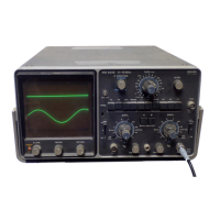
119
The
different
functions
of
the
logic
circuits
are
now
described
according
to the
horizontal
display
mode
selector
switch
S2;
-
When
no
pushbutton
is
depressed
or
when
MTB
is
depressed
flip-flop
D1609
is
set in
the
MTB
position
via
its R
and
S inputs
(output
10
is high).
The
MTB
pushbutton
releases
all
the
other
push-buttons
of
the
horizontal
deflection
mode
selector,
its
contacts
are
not
used.
In
the
MTB
position
of
switch
S2,
transistor
VI
509,
which
is driven
by
output
10 of flip-flop
D1609,
and
consequently
transistor
VI
511,
conduct.
Diode
gate
VI
51
3,
VI
51
4 is
therefore
opened
and
the
main
time-base
output
is
applied
via
transistor
VI
51
2
to
the X
amplifier,
via these
diodes
and
R1703.
In
this
mode
only
the main
time-base
sawtooth
signal
is fed
to the X
final
amplifier
and not
the
delayed
time-base
sawtooth
signal
and
the
X-deflection
signal.
-
With DTB
selected
flip-flop D1609
is set
to the DTB
state via its
S and R
inputs (output
1 1 is high)
.
In
the DTB
position
of switch
S2, transistor
VI
501
,
driven
by output
11 of
flip-flop
D1609 and
consequently
transistor
Vi 506
are
conducting.
The
diodes
VI
503 and
VI 504
conduct and
provide
a signal
path for the
output
sawtooth
signal of
the delayed
time-base
generator
to the
X final amplifier.
With DTB
selected
the main
time-base
signal
and the X
deflection
signal are
blocked.
EXT
X DEFL
—
In the EXT
X DEFL
position a
-t-5,2
V
is applied
via
switch
S2 to the base of
VI
516,
with
a result that the base
of VI 51
7 exceeds
+
5,2
V and this
transistor
is turned off.
Transistor
V1524
then starts
to conduct via R1528
and diode V1523
(8,2
V),
and
the external
signal for
amplifier VI
519,
VI
521
is routed via the
diode
gate
VI
522,
VI 526
to the X amplifier.
When EXT X DEFL
is
switched
off, transistor
VI
516 is turned off and
transistor
VI 517 conducts
via R1522.
The collector
of VI 517
is
therefore
at +5,2
V,
and as the
voltage across diode VI
523 is less
than
8,2
V, this diode
is blocked
and transistor VI 524
is turned off. In
this position the X MAGN
reed relay
K1 701 for the XI
,
XI
0,
may
be
switched
in. This
is not operative
when EXT
X DEFL is switched on.
ALT TB
—
With ALT TB
depressed, the oscilloscope is
set in the alternate
time-base
mode and the main
and delayed time-bases
are selected alternately.
ALT TB
is
not possible with DTB TIME/DIV
switch
Si 3 in
the "OFF"
position
and with
push-button
TRIG VIEW
of switch SI depressed.
Switching over from MTB
to
DTB
in ALT TB
mode is achieved by switching
in
transistor VI
509 and VI 501 in turn via flip-flop D1609.
In
ALT TB
a
+5
V signal is fed
to
input 4 of NAND D1606.
With the delayed
time-base switched
off and with TRIG VIEW
not depressed
a 0
V signal
appears
at output 6 of NAND D1606. With this
0
V
signal
NAND
D1608
(11-12-13)
is blocked and flip-flop D1609
is set for normal switching
by
its
clockpulse input signal. There is
no
longer
a
signal path
for the
alternate
signal from
the time-base generator
to
the
vertical display logic other
than
via
flip-flop
D
1609,
NAND 1608
(8-9-10)
and NAND
D1607
(8-9-10).
The flip-flop
output signal
is
also applied
to
R632
in the trace separation
circuit
to
control
the vertical space between
the two time-base displays.
 Loading...