Tel : 886-2-29162151
Fax: 886-2-29174598
VFD Driver/Controller IC PT6315
PT6315 v2.0 Page 5 Sep. 2002
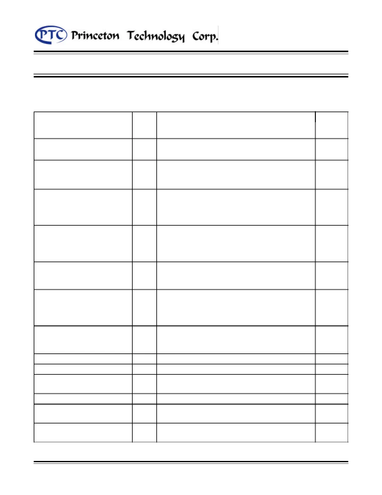
PIN DESCRIPTION
Pin Name I/O Description Pin No.
LED1 to LED4 O LED Output Pin 1 to 4
OSC I
Oscillator Input Pin
A resistor is connected to this pin to
determine the oscillation frequency
5
DOUT O
Data Output Pin (N-Channel, Open-Drain)
This pin outputs serial data at the falling
edge of the shift clock (starting from the
lower bit).
6
DIN
(Schmitt Trigger)
I
Data Input Pin
This pin inputs serial data at the rising edge
of the shift clock (starting from the lower
bit)
7
CLK
(Schmitt Trigger)
I
Clock Input Pin
This pin reads serial data at the rising edge
and outputs data at the falling edge.
8
STB
(Schmitt Trigger)
I
Serial Interface Strobe Pin
The data input after the STB has fallen is
processed as a command.
When this pin is "HIGH", CLK is ignored.
9
K1 to K2 I
Key Data Input Pins
The data inputted to these pins are latched
at the end of the display cycle.
10 ,11
VSS - Logic Ground Pin 12,44
VDD - Logic Power Supply 13,43
SG1/KS1 to SG16/KS16 O
High-Voltage Segment Output Pins
Also acts as the Key Source
14 to
29
VEE - Pull-Down Level 30
SG17/GR12 to SG24/GR5 O High Voltage Segment/Grid Output Pins
31 to
38
GR4 to GR1 O High-Voltage Grid Output Pins
39 to
42