1.1 Overview
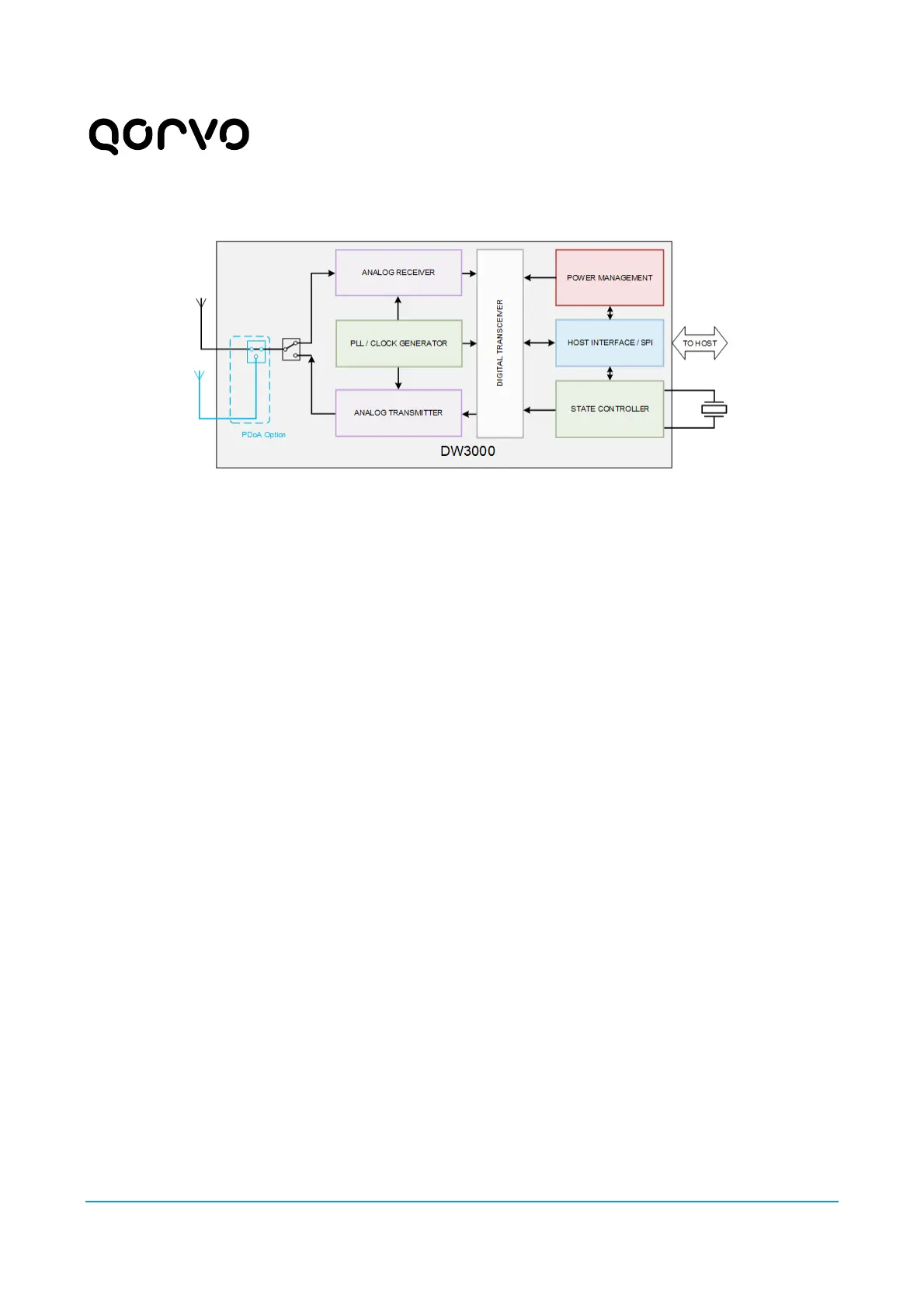
Figure 1: DW3000 high level function diagram
In any wireless communications system, the link budget is determined by several factors. These include:
• Transmitted power level
• Transmitter antenna gain
• Losses in the propagation channel (e.g. over the air)
• Receiver antenna gain
• Receiver sensitivity
QM33100 [1] and DW3000 [2] have a receiver sensitivity of between -92.6 dBm and -102.6 dBm depending
on the chosen configuration parameters (data rate), hardware setup (carrier frequency offset between TX and
RX nodes) and the acceptable system performance limits for particular applications (acceptable packet error
rate, for example).
The transmit output power of the QM33100 and DW3000 are limited by design to a maximum value of -31
dBm/MHz. This is more than adequate to meet the regulatory maximum limit of -41.3 dBm/MHz. That limit
applies in most countries where UWB is permitted and provides some margin to allow for PCB, temperature,
antenna and enclosure losses.
Although the QM33100 and DW3000 have an internal LNA, it is possible to improve the noise figure and
consequently the sensitivity of the receiver by adding an external LNA to the front end. Choosing an LNA with
a low noise figure and high gain is important.
The insertion of an LNA amplifier into the receiver path, between the antenna and the RF pins on the QM33100
and DW3000, can typically result in a 4 to 6 dB improvement in receiver sensitivity.
1.2 Hardware and Software Modifications
The QM33100/DW3000 has been designed to provide the necessary signals to control an external LNA. These
signals can control LNA power supply switching and RF switches to select between transmit and receive paths.
The hardware required is discussed in section 2 while the software modifications to enable the operation of
the external circuitry are discussed in section 3.
 Loading...