Reflex Service
Manual
Theory of Operation
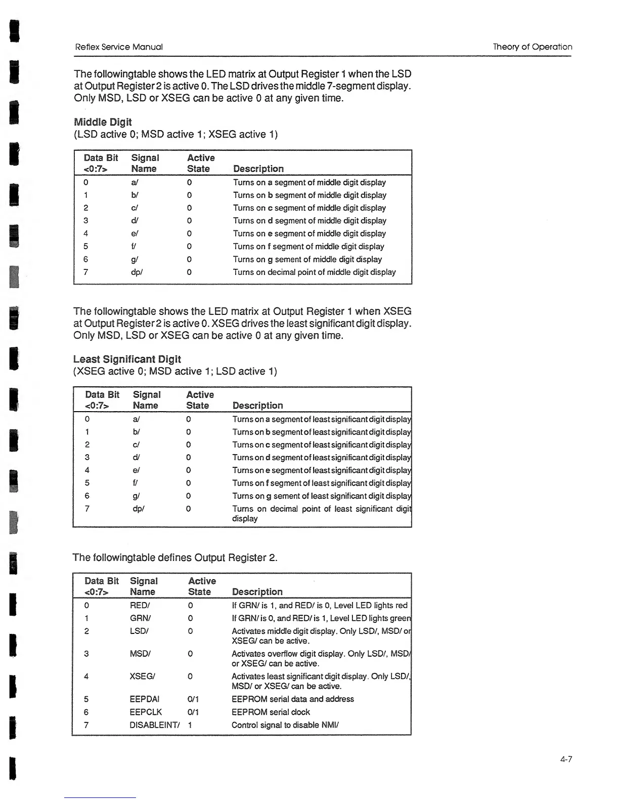
The followingtable shows
the
LED matrix
at
Output
Register
1 when
the
LSD
at Output
Register
2
is active
0. The LSD
drives the middle
7-segment
display.
Only
MSD, LSD
or XSEG can
be
active
0 at
any
given
time.
Middle
Digit
(LSD
active
0;
MSD
active
1
;
XSEG active
1)
Data
Bit
<0:7>
Signal
Name
Active
State
Description
0 a/ 0 Turns on a segment of middle digit display
1 b/
0 Turns on b segment of middle digit
display
2
of
0 Turns on c segment of middle digit display
3 d/
0
Turns
on
d
segment
of
middle digit display
4 8/ 0
Turns on
e
segment of middle digit display
5 f/ 0
Turns on
f
segment of
middle digit display
6
g/
0
Turns
on
g
sement of middle
digit display
7 dp/ 0 Turns on decimal point
of
middle digit display
The followingtable
shows the
LED
matrix
at Output
Register
1 when XSEG
at
Output
Register
2
is
active
0. XSEG
drives
the
least
significant digit
display.
Only MSD, LSD or
XSEG can
be
active
0 at
any
given
time.
Least
Significant Digit
(XSEG active
0;
MSD active
1
;
LSD
active
1)
Data Bit
Signal
Active
<0:7> Name
state
Description
0
a/ 0 Turns on a segment of least significant digit display
1
b/ 0
Turns
on b
segment
of
least
significant
digit display
2 c/
0 Turns on c segment of least significant digit display
3
d/ 0 Turns on d segment
of least
significant digit display
4
e/ 0 Turns on e segment of least significant digit
display
5 f/
0 Turns on f segment
of
least significant
digit
display
6
g/
0
Turns
on
g
sement of least significant digit
display
7 dp/ 0 Turns
on
decimal
point of least
significant digit
display
The
followingtable
defines
Output
Register
2.
Data Bit
<0:7>
Signal
Name
Active
State
Description
0
RED/ 0 If GRN/ is
1.
and RED/ is
0,
Level
LED
lights red
1 GRN/ 0
If GRN/ is
0,
and
RED/
is
1
,
Level
LED
lights green
2 LSD/ 0 Activates middle digit display. Only LSD/, MSD/ or
XSEG/
can be active.
3 MSD/ 0
Activates
overflow digit display. Only LSD/, MSD/
or XSEG/
can
be
active.
4
XSEG/
0
Activates least
significant digit display. Only LSD/,
MSD/
or
XSEG/ can be
active.
5
EEPDAI
0/1
Eeprom serial data and
address
6
EEPCLK 0/1
EEPROM
serial clock
7 DISABLEINT/
1
Control
signal
to
disable NMI/
4-7
 Loading...