EasyManua.ls Logo

Samsung MAX-485 - Page 31

Samsung MAX-485
69 pages
Print Icon
To Next Page IconTo Next Page
To Previous Page IconTo Previous Page
Loading...
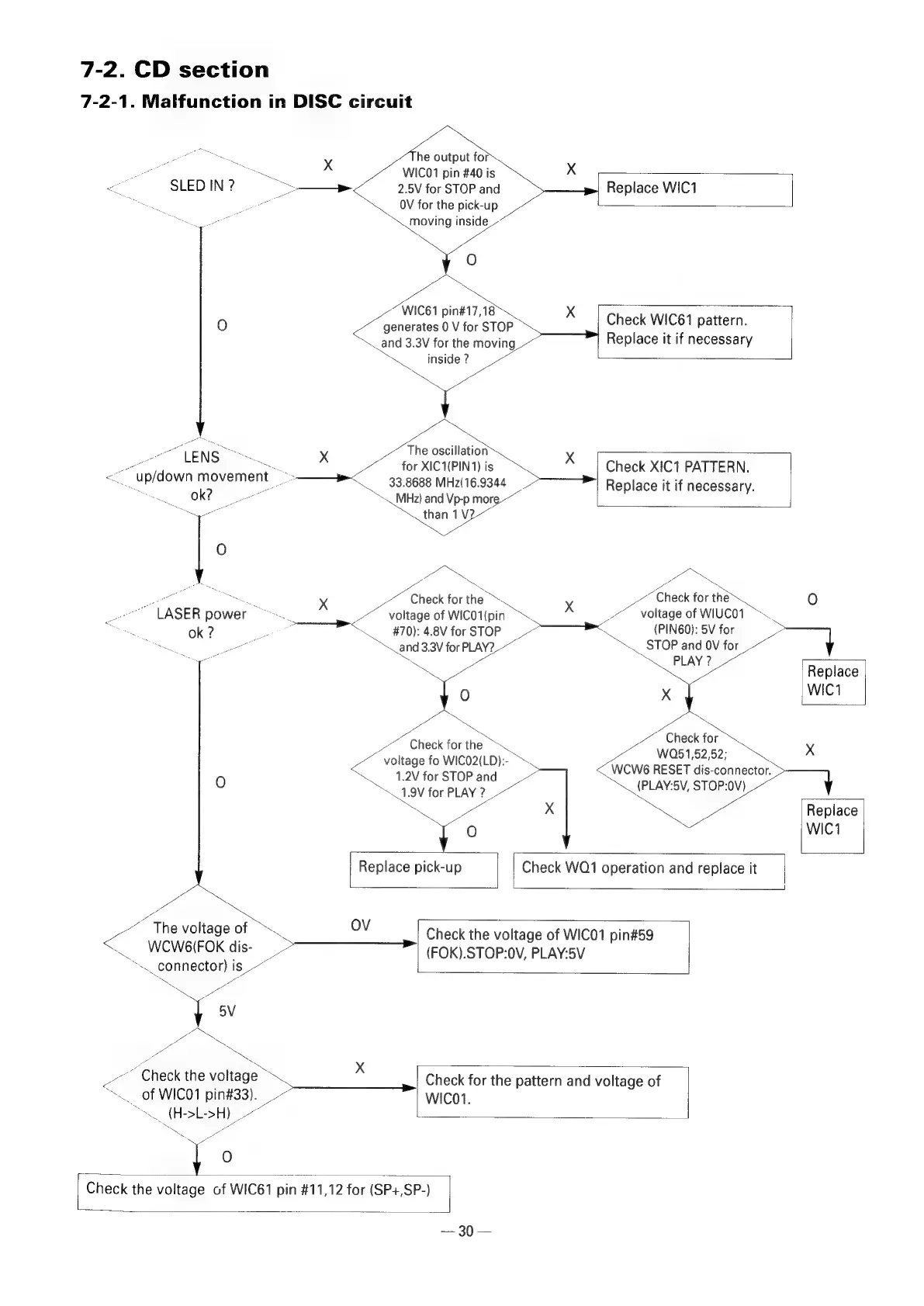
7-2.
CD
section
7-2-1.
Malfunction
in
DISC
circuit
SLED
IN
?
“LENS
Oke
~
LASER
power
~
ok
?
we
a
“The
voltage
of
WCWE6(FOK
dis-
“~
connector)
is
=
wer
=
ae
OY
sv
an
ae
PS
z
AS
~
~~
Check
the
voltage
~~
e
of
WICO1
pin#33).
™_
(H->L->H)
\
=
~~
for
XIC1(PIN1)
is
>
33.8688
MHz\16.9344
a
up/down
movement
—
>
he
output
for
WIC01
pin
#40
is
2.5V
for
STOP
and
OV
for
the
pick-up
moving
inside
we
WIC61
pin#17,18
<<
senerates
0
V
for
STOP
and
3.3V
for
the
moving
SS
inside
?
xX
X
_~
The
oscillation
Mhz)
and
Vp-p
mort
than
1
V?
vy
pis
xX
ZZ
Cheek
for
the
_~
voltage
of
WICO1pin
~~
x
o
ig
i
4.8V
for
STOP
and
3.3V
for
PLAY?
SY
ae
A
Cheek
for
te
‘voltage
fo
Le
1.2V
for
STOP
and
a
for
ee
te
ye
Replace
WIC1
X
Check
WIC61
pattern.
Replace
it if
necessary
Check
XIC1
PATTERN.
Replace
it
if
necessary.
Pa
xe
ie
~~
Check
for
the
@)
se
voltage
of
WIUCO1
(PIN60):
5V
for
oe
Replace
WIC1
Check
f
for
SS
W051,52,52;
SX
WCW6
RESET
dis-connector.
(PLAY:5V,
STOP:0V)
TSS
STOP
and
OV
for
PLAY
?
Replace
WIC1
|
Replace
pick-up
|
Check
WQ1
operation
and
replace
it
OV
Check
the
voltage
of
WICO1
pin#59
(FOK).STOP:0V,
PLAY:5V
X
WICO1.
Check
for
the
pattern
and
voltage
of
Check
the
voltage
of
WIC61
pin
#11,12
for
(SP+,SP-)
|