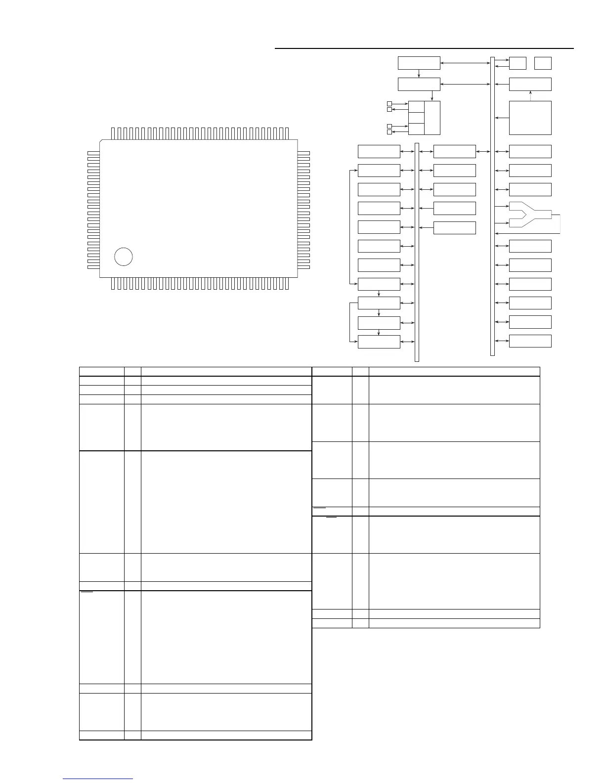
2/INT3/T0IN
S0/T
0
Interrupt Control
Standby Control
IR
ROM
PL
A
CF
RC
X’tal
Clock
Generator
PC
Base Ti
mer
SIO0
SIO1
Timer
0
Timer
1
AD
C
INT0 to 3
Noise Filtter
RAM
128 byte
s
Port 1
Port 3
Port 7
High
Voltage Output
VFD Co
ntroller
Bus In
terface ACC
B Register
C Register
PSW
RA
R
RA
M
St ack Poin te
r
Wa
tch dog Timer
Port 0
SI0 Automatic
transmission
ALU
Port 8
Pin Name I/O Function Description Pin Name I/O Function Description
VSS1,2 Power pin (-) * 1 S7/T7 to * Output for VFD display controller segment/timing with internal
VDD1,2,3,4 Power pin (+) * 1 S15/T15 pull-down resisitor in common.
VP Power pin (+) for the VFD output pull-down resist * Internal pull-down resistor output
* 8-bit input/output port S16 to S31 * Output for VFD display conroller segment
Input/output port * Other function
* Input for port 0 interrupt S16 ~ S23 : High voltage input port PC0 ~ PC7
* Inout for HOLD release S24 ~ S31 : High voltage input port PD0 ~ PD7
* 15V withstand at N-channel open drain output S32 to S47 * Output for VFD display conroller segment
* 8-bit input/output port * Other function
Input/output can be specified in bit unit S32 ~ S39 : High voltage input port PE0 ~ PC7
* Other pin functions S40 ~ S47 : High voltage I/O port PF0 ~ PD7
P10 : SIO0 data output S48 to S51 * Output for VFD display conroller segment
P11 : SIO0 data input/bus input/output * Other function
P12 : SIO0 clock input/output S48 ~ S51 : High voltage I/O port PG0 ~ PD3
P13 : SIO1 data ouput RES I Reset pin
P14 : SIO1 data input/bus input/output XT1/P74 I * Input pin for 32.768kHz crystal oscillation
P15 : SIO1 clock input/output * Other function
P16 : Buzzer output P74 for input port
P17 : Timer output (PWM0 output) Incase of non use, connect to VDD1
* 8-bit input/output port XT2/P75 O * Output pin for 32.768kHz crystal oscillation
Input/output in bit unit * Other function
* 15V withstand at N-channel open drain output P75 for input port
P70 - P73 I/O * 4-bit input/output port * In case of non use,
P74 - P75 I
Input/output port
At using as oscillator, should be left opened
* 2-bit input port
At using as a port, connect to VDD1
* Other pin functions
CF1 I Input pin for ceramic resonator oscillation
P70 : INT0 input/Hold release/N ch-Tr.
CF2 O Output pin for ceramic resonator oscillation
output for watchdog timer
P71 : INT1 input/ HOLD release input
* All of port options (except pull-up resistor of port 0) can be specified in bit unit.
P72 : INT2 input/timer 0 event input
* A state of pins at reset
P73 : INT3 input with noise filter/timer 0 event input
P74 : Input pin XT1 for 32.768kHz crystal resonator oscillation
P75 : Output pin XT2 for 32.768kHz crystal resonator oscillation
P80 - P83 I * 4-bit input/output port
P84 - P87 I/O Input/output in bit unit
* 4-bit input port
* Other function
AD input port (8 port pins)
S0/T0 to S6/T6 O Output for VFD display controller segment/timing in common
O
I/O
I/O
P30 - P37
I/OP00 - P07
I/OP10 -P17
 Loading...