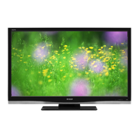
LC-37D90U
5 – 32
AG3, AH3, AJ3, AK3,
AH4, AG4, AG5, AH5,
AJ5, AK5
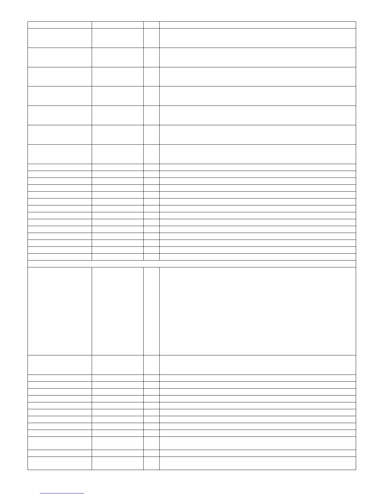
DP_B [19:10] I Digital input port B [19:10].
AK6, AJ6, AH6, AG6,
AG7, AH7, AJ7, AK7, AK8,
AJ8
DP_B [9:0] I Digital input port B [9:0].
AH9, AG9, AG10, AH10,
AJ10, AK10, AG11, AJ11,
AK11, AK12
DP_A [29:20] I/O Digital input port A [29:20] or Digital output port A [29:20].
AJ12, AH12, AG12, AG13,
AH13, AG14, AH14, AJ14,
AK14, AK15
DP_A [19:10] I/O Digital input port A [19:10] or Digital output port A [19:10].
AJ15, AG15, AK16, AJ16,
AH16, AG16, AG17,
AH17, AJ17, AK17
DP_A [9:0] I/O Digital input port A [9:0] or Digital output port A [9:0].
AG19, AH19, AJ19, AK19,
AK20, AJ20, AH20, AG20,
AG21, AH21
DP_C [9:0] I/O Digital input port C [9:0] of CCIR656/601 or CCIR601 output.
AG22, AG23, AH23, AJ23,
AK23, AH24, AG24,
AG25, AH25, AG26
DP_D [9:0] I/O Digital input port D [9:0] of CCIR656/601.
AH26 CLK_D I/O Digital port D CLK input.
AK21 CLK_C I/O Digital port C CLK input.
AK4 CLK_B I Digital port B CLK input.
AK13 CLK_A I/O Digital port A CLK input.
AK9 DE_B I DE input of Digital port B.
AH18 DE_A I/O DE input of Digital port A.
AH8 HS_B I Hsync input of Digital port B.
AK18 HS_A I/O Hsync input of Digital port A.
AG8 VS_B I Vsync input of Digital port B.
AJ18 VS_A I/O Vsync input of Digital port B.
AG18 FLD_A I/O Field input of Digital port A.
AJ9 FLD_B I Field input of Digital port B.
AK22 HS I/O Hsync output for Digital port.
AJ22 VS I/O Vsync output for Digital port.
Ball Assignments for Frame Buffer Memory.
B14, A14, C15, B15, C16,
D16, D17, C17, B17, A17,
C18, B18, C19, D19, D20,
C20, B20, A20, C21, B21,
C22, D22, D23, C23, B23,
A23, C24, B24, C25, D25,
D26, C26, K29, K30, L28,
L29, M28, M27, N27, N28,
N29, N30, P28, P29, R28,
R27, T27, T28, T29, T30,
U28, U29, V28, V27, W27,
W28, W29, W30, Y28,
Y29, AA28, AA27, AB27,
AB28
MD [63:0] I/O Memory data.
K28, K27, J27, J28, J30,
H30, H29, H28, G28, G29,
G30, F30
MA [11-0] I/O Memory Address.
A28 RAS# O RAS# signal powered by VDDH/VSS.
A27 CAS# O CAS# signal powered by VDDH/VSS.
B27 WE# O WE#, write enable signal powered by VDDH/VSS.
B28 CS1# O Chip select 0 for the first 2/4 Mbyte of SGRAM/SDRAM powered by VDDH/VSS.
C28 CS0# O Chip select 1 for the first 2/4 Mbyte of SGRAM/SDRAM powered by VDDH/VSS.
F29 MCK0 O Memory clock+.
B29 MCK1 O Memory clock+.
E30 MCK0# O Memory clock-.
A29 MCK1# O Memory clock-.
A16, A19, A22, A25, M30,
R30, V30, AA30
DQM [7:0] O Read/Write bytes enable powered by VDDH/VSS.
C27 CLKE O Memory clock enable.
A15, A18, A21, A24, L30,
P30, U30, Y30
DQS [7:0] I/O Memory data strobe.
Pin No. Pin Name I/O Pin Function