LC-37D90U
5 – 33
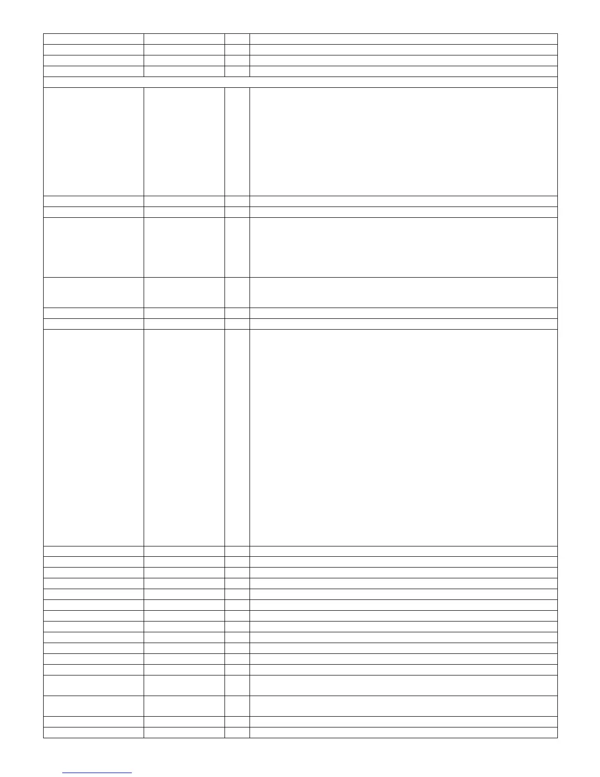
B30 MVREF --- DDR voltage reference.
A26 BA0 O Bank address select.
B26 BA1 O Bank address select.
Ball Assignments for Power and Ground.
A2, A3, A4, A5, B3, B4,
B5, B6, C4, C5, C6, D4,
D5, D6, E4, E5, E6, E7,
E8, E11,E12, E13, E18,
E19, E20, E21, F4, F5,
G4, G5, H5, J26, K26,
L26, M26, W26, Y26,
AA26, AC5, AD5, AE5,
AF5, AF6, AF7, AF8, AF9,
AF10, AF11, AF20, AF21,
AF22, AF23
VDDC --- 1.8V Digital core power.
C29, D21, V26 VSSR --- Digital Ground.
A30, E22, U26 VDDR --- Digital power for Memory.
C30, D28, D29, D30, E14,
E15, E16, E17, E23, E24,
E25, E26, E27, E28, E29,
F26, F27, F28, G26, G27,
H26, N26, P26, R26, T26,
AB26, AC26, AD26, AE26
VDDM ---
AF12, AF13, AF14, AF15,
AF16, AF17, AF18, AF19,
AF24, AF25
VDDH --- 3.3V Digital I/O power.
E9, E10, J5, K5 VDDH_CPU --- CPU I/O power 3.3V.
B7 V5SF --- 5V reference Tolerance voltage (Must be connected to 5V even in standby mode).
B16, B19, B22, B25, C14,
D15, D18, D24, D27, H27,
J29, L5, L27, M5, M12,
M13, M14, M15, M16,
M17, M18, M19, M29, N5,
N12, N13, N14, N15, N16,
N17, N18, N19, P12, P13,
P14, P15, P16, P17, P18,
P19, P27, R5, R12, R13,
R14, R15, R16, R17, R18,
R19, R29, T12, T13, T14,
T15, T16, T17, T18, T19,
U5, U12, U13, U14, U15,
U16, U17, U18, U19, U27,
V12, V13, V14, V15, V16,
V17, V18, V19, V29, W5,
W12, W13, W14, W15,
W16, W17, W18, W19, Y5,
Y27, AA5, AA29, AB5,
AC27, AC28, AF4, AF26,
AH11, AH15, AH22, AJ4,
AJ13, AJ21
VSS --- Digital ground.
AB4 DVSS --- Ground of ADC Digital circuit.
AC1 DVDD --- 1.8V power for ADC Digital circuit.
J3 AVSS_BG_ASS --- ADC ground.
J2 AVDD3_BG_ASS --- ADC power.
AD4 PAVDD1 --- Power for analog PLL (2.5V).
AE2 PAVSS --- PLL ground.
AD2 PAVSS1 --- Ground for analog PLL.
AC4 PAVSS2 --- Ground for analog PLL.
AE3 PAVDD --- PLL power.
AC2 PAVDD2 --- Power for analog PLL (2.5V).
AF3 PDVDD --- Power for analog PLL.
AE4 PDVSS --- PLL ground.
G2, R1, Y2, V2, L1 AVDD_ADC [56, 4,
3, 2, 1]
--- Power for analog ADC.
G3, T5, AA4, V5, L2 AVSS_ADC [56, 4,
3, 2, 1]
--- Ground for analog ADC.
AA3, M3 AVDD3_ADC [2, 1] ---
L3 AVDD3_OUTBUF --- 3.3V power for output.
Pin No. Pin Name I/O Pin Function
 Loading...