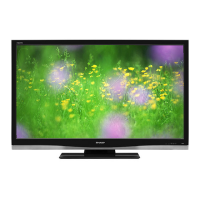
LC-37D90U
5 – 44
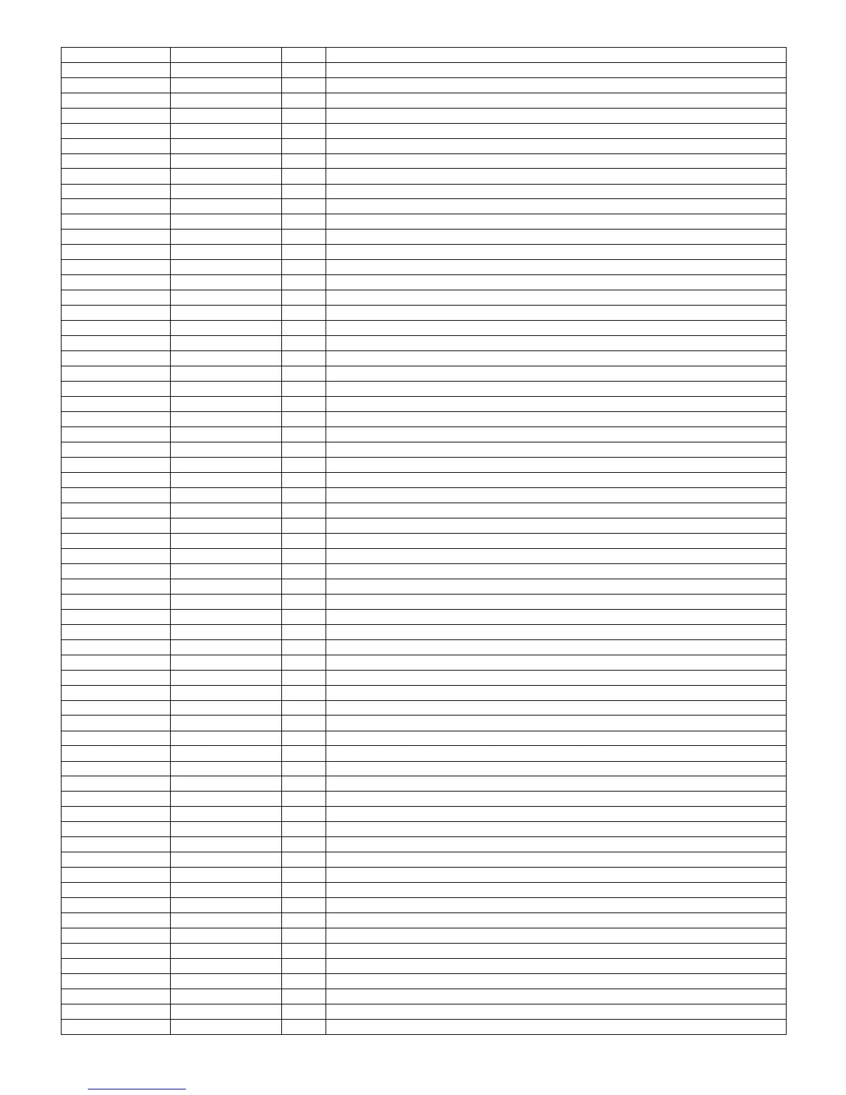
AM32 VIDINCBCR1 I External video data CB/CR input1. Shared with DBUGTPC1.
AM33 VIDINCBCR0 I External video data CB/CR input0.
AL23 HDOUT O Horizontal sync output.
AK24 VDOUT O Vertical sync output.
AK23 DOUTCLK O Display clock output.
AK22 DOUTY9 O Video Y output9 or Video G output9. Shared with PIO30.
AL22 DOUTY8 O Video Y output8 or Video G output8. Shared with PIO29.
AM22 DOUTY7 O Video Y output7 or Video G output7. Shared with PIO28.
AN22 DOUTY6 O Video Y output6 or Video G output6. Shared with PIO27.
AN21 DOUTY5 O Video Y output5 or Video G output5. Shared with PIO26.
AM21 DOUTY4 O Video Y output4 or Video G output4. Shared with PIO25.
AL21 DOUTY3 O Video Y output3 or Video G output3. Shared with PIO24.
AK21 DOUTY2 O Video Y output2 or Video G output2. Shared with PIO23.
AK20 DOUTY1 O Video Y output1 or Video G output1. Shared with PIO22.
AL20 DOUTY0 O Video Y output0 or Video G output0. Shared with PIO21.
AM20 DOUTPB9 O Video PB output9 or Video B output9. Shared with PIO32.
AN20 DOUTPB8 O Video PB output8 or Video B output8. Shared with DBUGPCST8.
AN19 DOUTPB7 O Video PB output7 or Video B output7. Shared with DBUGPCST7.
AM19 DOUTPB6 O Video PB output6 or Video B output6. Shared with DBUGPCST6.
AL19 DOUTPB5 O Video PB output5 or Video B output5. Shared with DBUGPCST5.
AK19 DOUTPR4 O Video PB output4 or Video B output4. Shared with DBUGPCST4.
AK18 DOUTPR3 O Video PB output3 or Video B output3. Shared with DBUGPCST3.
AL18 DOUTPB2 O Video PB output2 or Video B output2. Shared with DBUGPCST2.
AM18 DOUTPB1 O Video PB output1 or Video B output1. Shared with DBUGPCST1.
AN18 DOUTPB0 O Video PB output0 or Video B output0. Shared with DBUGPCST0.
AN17 DOUTPR9 O Video PR output9 or Video R output9. Shared with PIO31 and VCRDOUT7.
AM17 DOUTPR8 O Video PR output8 or Video R output8. Shared with DBUGTCK and VCRDOUT6.
AL17 DOUTPR7 O Video PR output7 or Video R output7. Shared with DBUGDCLK and VCRDOUT5.
AK17 DOUTPR6 O Video PR output6 or Video R output6. Shared with DBUGTDO and VCRDOUT4.
AK16 DOUTPR5 O Video PR output5 or Video R output5. Shared with DBUGTDI and VCRDOUT3.
AL16 DOUTPR4 O Video PR output4 or Video R output4. Shared with DBUGTMS and VCRDOUT2.
AM16 DOUTPR3 O Video PR output3 or Video R output3. Shared with DBUGTRST_N and VCRDOUT1.
AN16 DOUTPR2 O Video PR output2 or Video R output2. Shared with DBUGTPC3 and VCRDOUT0.
AN15 DOUTPR1 O Video PR output1 or Video R output1. Shared with DBUGTPC2.
AM15 DOUTPR0 O Video PR output0 or Video R output0. Shared with DBUGTPC1.
AM23 FLPH O Frame field.
AN23 HBLANK O Horizontal blanking signal.
AN24 VBLANK O Vertical blanking signal.
AM24 BGATE O Black level ID zone specifying signal.
AL24 YS O Video Graphic ID signal.
AK25 DCLKI74M I 74MHz clock input for HD.
AL25 DCLKI54M I 54MHz clock input for SD.
AN26 DCLKICAP I Clock input for capture 74M/54M.
AM25 PWM74M O PWM for 74MHz clock.
AN25 PWM54M O PWM for 54MHz clock.
AK26 VCRCLKO O Clock output for ‘VCR standard digital video output’.
AE31 YOUT O YOUT for playback.
AF31 PBOUT O PBOUT for playback.
AG31 PROUT O PROUT for playback.
AA31 VCRYOUT O VOUT for recording.
AB31 VCRCOUT O COUT for recording.
AC31 VCRCVOUT O CVBS OUTPUT for recording.
AE32 YNEG O YOUT inversed signal for playback should be connect pull-down resister.
AF32 PBENG O PBOUT inversed signal for playback should be connect pull-down resister.
AG32 PRNEG O PROUT inversed signal for playback should be connect pull-down resister.
AA32 VCRYNEG O YOUT inversed signal for recording should be connect pull-down resister.
AB32 VCRCNEG O COUT inversed signal for recording should be connect pull-down resister.
AC32 VCRCVNEG O CVBS OUT inversed signal for recording should be connect pull-down resister.
AL28 HSYNC O Horizontal sync.
AM28 VSYNC O Vertical sync.
AK28 FASTBLK O Fast Blanking signal.
AN27 CSYNC1 O Composite sync1.
AN28 CSYNC0 O Composite sync0.
D16 CLKX12 I PLL for Micro processor.
Pin No. Pin Name I/O Pin Function