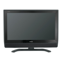
LC-37D90U
5 – 53
L14 HSDI1_DVALIDz
(HSDI1_Enz)
I/O HSDI port 1 data Valid pin. This pin indicates if data on the HSDI data bus is valid for reading or writ-
ing.
For transmit onto 1394, this signal is input to the RH-IXB323WJZZQ by the system with the data.
For receive from 1394, the RH-IXB323WJZZQ outputs this signal with the data.
If not used in transmit mode, this signal can be tied low.
HSDI port 1 enable pin (HSDI1_Enz) in HSDI RX mode 8/9 (celynx sync mode B compatible
modes).
This signal is always an input in HSDI RX mode 8/9. This signal indicates whether data can be drive
onto the HSDI bus. (i.e. if HSDI1_Enz is disserted, HSDI1 data bus and HSDI1 sync will be tri-
stated).
L13 HSDI1_ERRORz
(HSDI1_FrameSyncz)
I/O HSDI port 1 Error pin in MPEG2-DSS mode. This signal is used to indicate the value of the TS error
bit in the 10 bytes DSS header.
HSDI1_Frame Sync pin HSDI DV mode (TX modes 6/7, RX modes 6-9). This signal is used to indi-
cate the start of DV frames.
This pin is not used in MPEG2-DVB mode. This signal can be left open when HSDI1 is programmed
for RX direction (1394 RX) only. This signal should be pulled up/down when HSDI1 is programmed
for TX direction (1394 TX) or used for both directions.
H12 HSDI1_D0 I/O HSDI port 1 data 0 pin. Data 0 is the least significant bit on the HSDI data bus.
In serial mode, only HSDI1_D [0] is used, HSDI1_D [7:1] are not used.
H13 HSDI1_D1 I/O HSDI port 1 data 1 pin. In HSDI transmit serial mode (1394 TX), HSDI1_D [7:1] are in don't care sta-
tus. In HSDI receive serial mode (1394 RX), HSDI1_D [7:1] are Hi-Z. In serial mode, HSDI1_D [7:1]
can be tied directly to GND.
H11 HSDI1_D2 I/O HSDI Port 1 Data 2 Pin.
(For serial mode operation, see PIN description for HSDI1_D1 above.)
J10 HSDI1_D3 I/O HSDI Port 1 Data 3 Pin.
(For serial mode operation, see PIN description for HSDI1_D1 above.)
J14 HSDI1_D4 I/O HSDI Port 1 Data 4 Pin.
(For serial mode operation, see PIN description for HSDI1_D1 above.)
J13 HSDI1_D5 I/O HSDI Port 1 Data 5 Pin.
(For serial mode operation, see PIN description for HSDI1_D1 above.)
J12 HSDI1_D6 I/O HSDI Port 1 Data 6 Pin.
(For serial mode operation, see PIN description for HSDI1_D1 above.)
K14 HSDI1_D7 I/O HSDI Port 1 Data 7 Pin. Data 7 is the most significant bit on the HSDI data bus.
(For serial mode operation, see PIN description for HSDI1_D1 above.)
HSDI2
Note: If this port is not used, all HSD1 signals can be tied to GND as long as HSDI2Cfg. Enable is set to 0.
M11 HSDI2_CLKz I/O HSDI Port 2 clock. All signals and data on HSDI port 2 are clocked using this clock.
N11 HSDI2_SYNCz I/O HSDI Port 2 Synchronization signal is used to indicate the start of packet (or MPEG2 cell.)
For transmit onto 1394, this signal is input to the RH-IXB323WJZZQ from the system with the data.
For receive from 1394, the RH-IXB323WJZZQ outputs this signal with the data.
If not used in transmit mode, this signal can be tied low.
P13 HSDI2_DVALIDz
(HSDI2_Enz)
I/O HSDI Port 2 Data Valid Pin This pin indicates if data on the HSDI data bus is valid for reading or writ-
ing.
For transmit onto 1394, this signal is input to the RH-IXB323WJZZQ from the system with the data.
For receive from 1394, the RH-IXB323WJZZQ outputs this signal with the data.
If not used in transmit mode, this signal can be tied low.
HSDI port 2 enable pin (HSDI2_ENz) in HSDI RX mode 8/9 (ceLynx Sync mode B compatible
modes).
This signal always an input in HSDI RX mode 8/9. This signal indicates whether data can be driven
onto the HSDI bus. (i.e. if HSDI2_ENz is disserted, HSDI2 data bus and HSDI2_Sync will be tri-
stated).
N12 HSDI2_ERRORz
(HSDI2_FrameSyncz)
I/O HSDI Port 2 Error pin in MPEG2-DSS mode. This signal is used to indicate the value of the TS error
bit in the 10 bytes DSS header.
HSDI2_Frame Sync pin in HSDI DV mode (TX Modes 6/7, RX Modes 6-9). This signal is used to
indicate the start of DV frames.
This pin is not used in MPEG2-DVB mode. This signal can be left open when HSDI2 is programmed
for RX direction (1394 RX) only. This signal should be pulled up/down when HSDI2 is programmed
for TX direction (1394 TX) or used for both directions.
P12 HSDI2_D0 I/O HSDI1 port 2 Data 0 pin.
HSDI port 2 only supports serial data. HSDI2_D0 is the only data pin.
GPIO (General-Purpose Input/Output)
P10 GPIO0 I/O GPIO. Output is controlled by the internal register.
Input is monitored by internal register.
Can be used as watermark for also buffer 0.
L11 GPIO1 I/O GPIO. Output is controlled by the internal register. Input is monitored by internal register.
For HSDI0 RX mode 8/9 (ceLynx Sync mode B compatible), it can be configured for HSDI0 AV out-
put.
Pin No. Pin Name I/O Pin Function