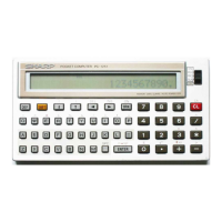
4
Pin Signal
I
N/OUT
Description (Standby
=
power
off)
No.
name
1
A01 OUT
Address
bus
,
high during standby
.
2
R/W OUT
Write clock, normally
high
.
3
0AL
OUT
Low order bits address latch, normally
h
i
gh. The clock used
to
latch
low
order 8 bits
of
16-b
i
t
address signal on the data bus line
when
a
larae caoacltv ROM
i
s
used.
4
TES
IN
Test pin, normally
low
.
5
01
IN
Oscillator
i
nput
.
6
00
OUT Oscillator output.
7
RES
IN
Reset input, active
h
i
gh
.
Normally, pulled down to low level.
8
Xin
IN Input (MT in)
of
microcassette signal from the CE-125 option.
9 ON IN
ON (BREAK) key input, normally pulled down to low level.
10
Xout
OUT Output (MT out
1)
of
m
i
crocassette signal to the CE-125 option and the buzzer.
11
D
i
s
OUT
LCD
dr
i
ver
con
t
rol signal.
12
HA
OUT LCD driver clock, low during standby and in
2
kHz oscillation during display.
•CPU pin
No
.
and
s
i
gnal description
1
1
0
P
O
R
T
1-4
KEY
OUT
5-8 for
TERMINAL
INTER FACE
F01
·
1
1
F
Out
Por
t
F0
2
:
!I
F
Out Port
FO
i
.
RAM
Bas
i
c
RAM
F
O
,
GRAOE
U
P
RAM
F
O;
.
PROGRAM ROM
C
E
Addre
ss
Latch
1
8
1
-B
¢
AL
R
/
W
F
01
F
01
F
03
F
04
FO
;
C
C
E
)(
C E
J
C
C
E )
I
,
1
I
B
•
!
xL
h
:~.
.
s
U
j
RO
M
(
BK
B
y
te
)
07
DO
•
C
.
P
.
U
.
(SC61860A02) ·········
8
Bits C-MOS
C
.
P
.
U
.
4. C.P.U.iNTERNAL
BLOCK DiAGRAM
&
TERMiNAL DESCRiPTiONS
Hg
-1
5