-
4
-
P
i
n
Signal
In/Out
F
u
nction
(standby
-
power
off)
No. Name
4
1
H10 Out
L
CD backplate
signal
,
high impedance
dur
i
ng
standby
,
but 4 level pulse issued
dur
i
ng
displaying.
4
2
H11
Out
LCD backplate
s
ignal, high impedance during standby, but 4 level pulse issued
dur
i
ng
displaying.
43
H12
Out
L
CD backplate
signal
,
high impedance during standby, but 4 level pulse issued during
display
i
ng
.
4
4 H13
Out
L
CD backplate
signal
,
high impedance
dur
i
ng
standby, but 4 level pulse
i
ssued
during
display
in
g
.
4
5 H14
Out
L
CD backplate
signal
,
high
i
mpedance during standby, but 4 level pulse issued during displaying.
46
H15
-
N
ot used because the display
unit
of this model
is
operates under
1
/
14
duty.
47
H16
-
N
o
t
used because the display
unit of
this model
i
s
operates under
1
/
14
duty.
4
8
VB
I
n
L
CD power supply, high during standby and VB when clock
is
at stop.
49
VD
i
S
In
L
CD power supply, high during standby and low when clock
is
at stop.
50
v cc
I
n
L
CD power supply, normally low.
5
1
vo
e
O
ut
L
CD
power supply, high during standby and low when clock
is
at stop.
52 VGG
I
n
Power supply, normally low
5
3
08
I
n
/
Out
D
a
ta bus line, normally high impedance
54
o7
I
n
/
Out
D
at
a
bus
line
,
normally high impedance
5
5
0
6
In/Out
Data bus
line
,
normally high impedance
5
6
o5
I
n
/
Out
Data bus
l
ine
,
normally high
i
mpedance
57
o4
I
n
/
Out
Data bus
line
,
normally high impedance
5
8
o
3
I
n
/
Out Data bus line, normally
h
i
gh
impedance
5
9
o
2
I
n
/
Out
D
ata
b
us
l
i
ne
,
normally high impedance
60
o
1
I
n
/
Out Data bus
line
,
normally high impedance
61
Fo5
Out
32
K ROM chip enable
62 Fo4
O
ut Option RAM chip
enab
l
e
6
3 Fo3
O
ut
LC
D driver LSI
(D
I
SPLAY
1)
chip enable
6
4 Fo2
Ou
t
D
ata ou
t
(Dout
)
peripheral data out
p
o
r
t outp
u
t
6
5
Fo1 Out
B
USY
(
1
/
F) out
port output
6
6 Bo8
O
ut LCD
dri
ver LSI (DISPLAY 2) chip enable
67
Bo
7
Out
(
A
1
4
)
add
r
ess
bus
lin
e
,
h
i
gh
during
stand
by
68 Bo6 Out
(
A 13)
addre
s s
bus
l
ine, high during standby
69 Bo5
Ou
t
(
A 12) address bus
l
ine
,
high
dur
i
ng
standb
y
70 Bo4
O
ut
(
A11) address bus
line
,
high during standby
71
Bo3
Out
(
A10) address bus
line
,
high during standby
72
Bo2 Out
(
A9) address bus line, high during standby
7
3
Bo1
Out
(
AB) addre
s
s
bus
l
ine
,
h
i
gh
during standby
7
4 Ao8 Out
(
A7) address bus
line
,
high during standby
75
Ao7 Out
(A6) address bus line,
h
i
gh
during
s
tandby
76 Ao6
Out
(
A5) address bus
line
,
high during standby
77
Ao5 Out
(
A4) address bus
line
,
high during standby
78
Ao4
Out
(A3) address bus line, high during standby
79 Ao3 Out
(A2) address bus
l
ine
,
high during
standb
y
80
Ao2 Out
(A1) address bus line, high during standby
-
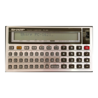
PC-1260
PC
-
1261