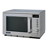
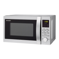
23
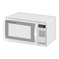
R-22AM
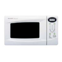
R-23AM
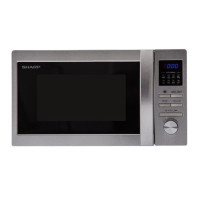
R-23AT
24 P31 IN Signal synchronized with commercial power source frequency.
This is basic timing for all time processing of LSI.
25 P30 OUT Terminal not used.
26 CNVSS IN Connected to Vc.(-5V)
27 RESET IN Auto clear terminal.
Signal is input to reset the LSI to the initial state when power is supplied. Temporarily
set to "L" level the moment power is supplied, at this time the LSI is reset. Thereafter
set at "H" level.
28 XIN IN Internal clock oscillation frequency setting input.
The internal clock frequency is set by inserting the ceramic filter oscillation circuit with
respect to XOUT terminal.
29 XOUT OUT Internal clock oscillation frequency control output.
Output to control oscillation input of XIN.
30/31
XCIN/XCOUT
IN/OUT Terminal not used.
32 VSS IN Power source voltage: -5V.
VC voltage of power source circuit input.
33 ø OUT Terminal not used.
34 R3 IN Signal coming from touch key.
When either one of G-12 line keys on key matrix is touched, a corresponding signal
out of P11, P12, P14 - P17 will be input into R3. When no key is touched, the signal
is held at "L" level.
35 R2 IN Signal similar to R3.
When either one of G-11 line keys on key matrix is touched, a corresponding signal
will be input into R2.
36 R1 IN Signal similar to R3.
When either one of G-10 line keys on key matrix is touched, a corresponding signal
will be input into R1.
37 R0 IN Signal similar to R3.
When either one of G-9 line keys on key matrix is touched, a corresponding signal
will be input into R0.
38 VP IN Anode (segment) of Fluorescent Display light-up voltage: -31V.
Vp voltage of power source circuit input.
39 P17 OUT Segment data signal.
The relation between signals and indicators are as follows:
Signal Segment Signal Segment
P24...................... i P13 .........................f
P23................... j,k P12 ........................e
P17.................. LB P11 ........................d
P16..................UB P10 ........................ c
P15.....................h P07 ........................b
P14.....................g P06 ........................a
Key strobe signal.
Signal applied to touch-key section. A pulse signal is input to R0 - R3 terminal while
one of G-6 line keys on key matrix is touched.
40 P16 OUT Segment data signal. Signal similar to P17.
Key strobe signal.
Signal applied to touch-key section. A pulse signal is input to R0 - R3 terminal while
one of G-5 line keys on key matrix is touched.
41 P15 OUT Segment data signal. Signal similar to P17.
Key strobe signal.
Signal applied to touch-key section. A pulse signal is input to R0 - R3 terminal while
one of G-4 line keys on key matrix is touched.
Pin No. Signal I/O Description
H : GND
L (-5V)
20 msec
GND
-31(V)
ß(50Hz)