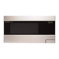
27
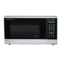
R-430DK
R-430DW
R-430DQ
R-440DK
R-440DW
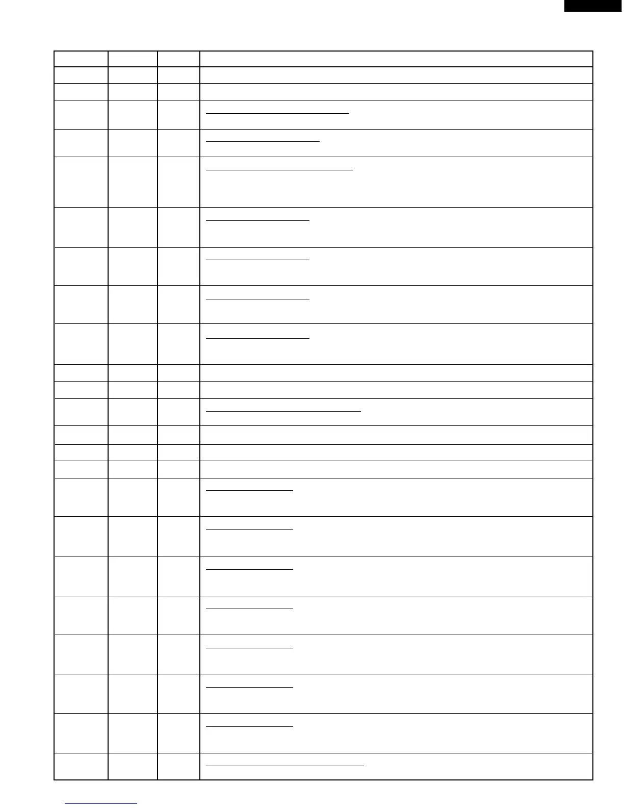
1 TIOCA2 OUT Terminal not used.
2 A20 OUT Terminal not used.
3 Vcc IN Power source voltage : +5.0V.
The power source voltage to drive LSI is input to Vcc terminal. Connected to Vcc.
4 TMO0 OUT Signal to sound buzzer.
A: key touch sound (short beep). B: Completion sound (melody or long beep).
5 PB1 IN Signal coming from touch key.
When either G11 line on key matrix is touched, a corresponding signal out of P93,
P94, P95, P40, P41, P42, P43 and P44 will be input into PB1. When no key is
touched, the signal is held at "H" level.
6 PB2 IN Signal similar to PB1.
When either G12 line on key matrix is touched, a corresponding signal will be input
into PB2.
7 PB3 IN Signal similar to PB1.
When either G13 line on key matrix is touched, a corresponding signal will be input
into PB3.
8 PB4 IN Signal similar to PB1.
When either G6 line on key matrix is touched, a corresponding signal will be input
into PB4.
9 PB5 IN Signal similar to PB1.
When either G5 line on key matrix is touched, a corresponding signal will be input
into PB5.
10-11 PB6-PB7 OUT Terminal not used.
12 RESO OUT Terminal not used.
13 Vss IN Power source voltage: GND(0V).
The power source voltage to drive LSI is input to Vss terminal.
14 TxD0 OUT Data signal is output to a memory IC (IC4).
15 P91 OUT Clock signal is output to a memory IC (IC4).
16 RxD0 OUT Terminal not used.
17 P93 OUT Key strobe signal.
Signal applied to key unit section. A pulse signal is input to PB1-PB5 terminal while
one of G1 line keys on key matrix is touched.
18 P94 OUT Key strobe signal.
Signal applied to key unit section. A pulse signal is input to PB1-PB5 terminal while
one of G2 line keys on key matrix is touched.
19 P95 OUT Key strobe signal.
Signal applied to key unit section. A pulse signal is input to PB1-PB5 and AN1
terminal while one of G3 line keys on key matrix is touched.
20 P40 OUT Key strobe signal.
Signal applied to key unit section. A pulse signal is input to PB1-PB5 terminal while
one of G14 line keys on key matrix is touched.
21 P41 OUT Key strobe signal.
Signal applied to touch screen section. A pulse signal is input to PB1-PB5 terminal
while one of G7 line keys on key matrix is touched.
22 P42 OUT Key strobe signal.
Signal applied to touch screen section. A pulse signal is input to PB1-PB5 terminal
while one of G8 line keys on key matrix is touched.
23 P43 OUT Key strobe signal.
Signal applied to touch screen section. A pulse signal is input to PB1-PB5 terminal
while one of G9 line keys on key matrix is touched.
24 Vss IN Power source voltage : GND(0V).
The power source voltage to drive LSI is input to VSS terminal.
LSI(IXA029DR) : R-440DK/DW
The I/O signal of the LSI(IXA029DR) is detailed in the following table.
Pin No. Signal I/O Description