Understanding the Hardware | Preparing for first use
2
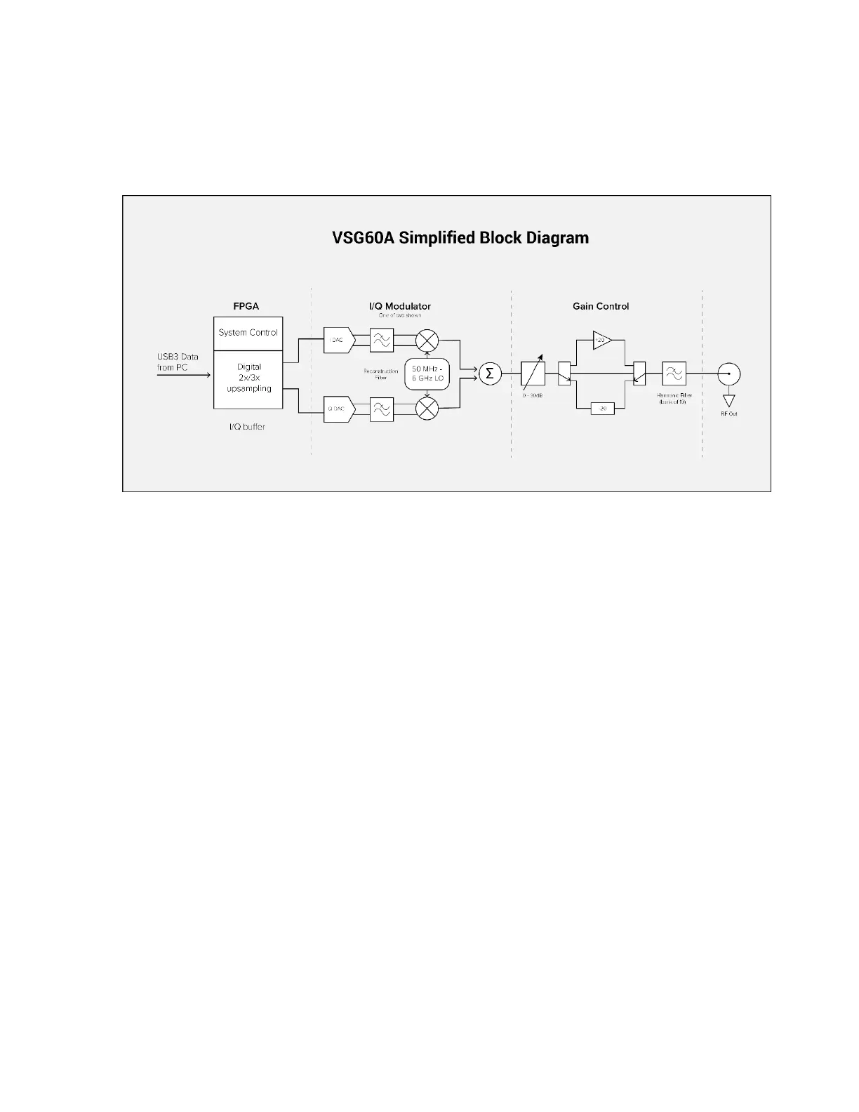
2 Understanding the Hardware
At the heart of the VSG60A is pair of quadrature modulators, one for below 2 GHz, and one for above
2 GHz (and a small segment around 800 MHz), driven by a dual channel DAC. The DAC clocks in
I/Q samples at 66-102.4 MSPS. The data rate from the PC to the FPGA is 22-51.2 MSPS I/Q, so
inside the FPGA we digitally up-sample by a factor of 2 or 3. This allows the use of a single optimized
reconstruction filter for typically better than 60 dB rejection of any aliased baseband signals, and
allows the PC to efficiently up-sample the user-selected baseband clock rate by a simple power of
two.
The baseband clock is generated from a 2.4 to 2.8 GHz VCO and divided down to 66-102.4 MHz.
Standard telecom symbol rates can be produced with 0 ppm additive error, and any symbol rate can
be produced with less than 1 ppm error.
The local oscillator (LO) generates a low phase noise CW signal (typically -125 dBc/Hz at a 10 kHz
offset from 1 GHz) for the I/Q modulators. Below 2 GHz, the LO runs at twice the RF frequency and
is digitally divided into quadrature. Above 2 GHz, a polyphase filter generates the quadrature LO for
the mixers. The LO switches frequencies in 200 microseconds for frequency-hopping applications.
The LO has 1/6 Hz resolution when digital tuning is disabled, and better than 1 µHz when digital tuning
is enabled. See the section on digital tuning for more information.
Both the baseband clock and LO are synthesized from a low phase noise 80 MHz clock, tied to either
the internal 10 MHz voltage-controlled, temperature-compensated crystal oscillator (VCTCXO), or the
user’s external 10 MHz input.
From the modulators, up to 20 dB of gain or 50 dB of attenuation is applied, in 2 dB steps. The
VSG60A software typically automatically selects the best setting based on output amplitude, but
 Loading...